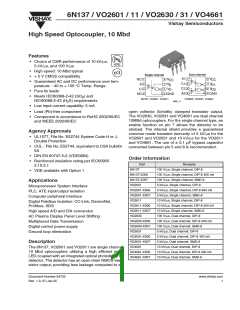
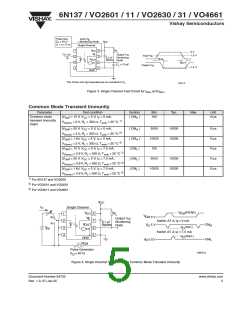
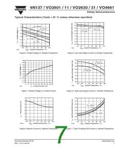
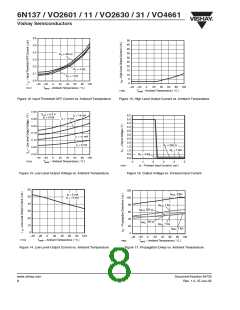
6N137 / VO2601 / 11 / VO2630 / 31 / VO4661
Vishay Semiconductors
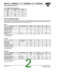
Truth Table (Positive Logic)
LED
ENABLE
OUTPUT
ON
H
H
L
H
H
H
L
OFF
ON
L
OFF
ON
L
NC
NC
OFF
H
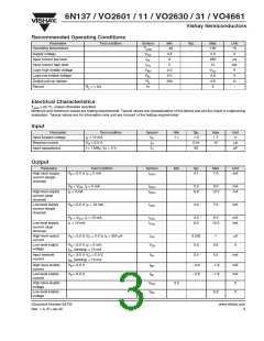
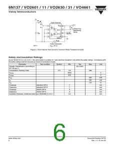
Absolute Maximum Ratings
Tamb = 25 °C, unless otherwise specified
Stresses in excess of the absolute Maximum Ratings can cause permanent damage to the device. Functional operation of the device is
not implied at these or any other conditions in excess of those given in the operational sections of this document. Exposure to absolute
Maximum Rating for extended periods of the time can adversely affect reliability.
Input
Parameter
Average forward current1)
Test condition
Symbol
IF
Value
Unit
mA
20
Average forward current2)
Reverse input voltage
IF
VR
VE
IE
15
mA
V
5
Enable input voltage1)
Enable input current1)
Surge current
VCC + 0.5 V
V
5
mA
mA
t = 100 µs
IFSM
200
1) Package: Single DIP-8
2) Package: Dual DIP-8
Output
Parameter
Test condition
1 minute max.
Symbol
Value
Unit
Supply voltage
VCC
7
V
Output current
Output voltage
IO
50
7
mA
V
VO
PO
PO
Output power dissipation1)
Output power dissipation2)
1) Package: Single DIP-8
2) Package: Dual DIP-8
85
60
mW
mW
Coupler
Parameter
Test condition
Symbol
Tstg
Value
Unit
°C
Storage temperature
- 55 to + 150
Operating temperature
Tamb
- 40 to + 100
260
°C
°C
Lead solder temperature1)
Solder reflow temperature2)
Isolation test voltage
for 10 sec.
for 1 minute
t = 1.0 sec.
260
°C
VISO
5300
VRMS
1) Package: DIP-8 through hole
2) Package: DIP-8 SMD
www.vishay.com
2
Document Number 84732
Rev. 1.0, 07-Jun-05

 VISHAY [ VISHAY ]