6N137 / VO2601 / 11 / VO2630 / 31 / VO4661
Vishay Semiconductors
Recommended Operating Conditions
Parameter
Test condition
Symbol
Tamb
Min
- 40
Typ.
Max
100
Unit
°C
Operating temperature
Supply voltage
VCC
IFL
4.5
0
5.5
250
15
V
µA
mA
V
Input current low level
Input current high level
Logic high enable voltage
Logic low enable voltage
Output pull up resistor
Fanout
IFH
VEH
VEL
RL
5
2.0
0.0
330
VCC
0.8
4 K
5
V
Ω
RL = 1 kΩ
N
-
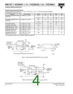
Electrical Characteristics
Tamb = 25 °C, unless otherwise specified
Minimum and maximum values are testing requirements. Typical values are characteristics of the device and are the result of engineering
evaluation. Typical values are for information only and are not part of the testing requirements.
Input
Parameter
Test condition
IF = 10 mA
R = 5.0 V
Symbol
Min
1.1
Typ.
1.4
Max
1.7
Unit
Input forward voltage
VF
V
Reverse current
V
IR
0.01
55
10
µA
Input capacitance
f = 1 MHz, VF = 0 V
CI
pF
Output
Parameter
Test condition
Symbol
ICCH
Min
Typ.
4.1
Max
7.0
Unit
mA
High level supply
current (single
channel)
V
V
E = 0.5 V, IF = 0 mA
E = VCC, IF = 0 mA
ICCH
ICCH
3.3
6.9
6.0
mA
mA
High level supply
current (dual
channel)
IF = 0 mA
12.0
Low level supply
current (single
channel)
V
E = 0.5 V, IF = 10 mA,
ICCL
4.0
7.0
mA
V
E = VCC, IF = 10 mA
ICCL
ICCL
3.3
6.5
6.0
mA
mA
Low level supply
current (dual
channel)
IF = 10 mA
12.0
High level output
current
V
E = 2.0 V, VO = 5.5 V, IF = 250 µA
IOH
0.002
0.2
1
µA
Low level output
voltage
VE = 2.0 V, IF = 5 mA,
VOL
0.6
V
IOL (sinking) = 13 mA
Input treshold
current
V
E = 2.0 V, VO = 5.5 V,
ITH
2.4
5.0
mA
IOL (sinking) = 13 mA
High level enable
current
VE = 2.0 V
IEH
IEL
- 0.6
- 0.8
- 1.6
- 1.6
mA
mA
V
Low level enable
current
VE = 0.5 V
High level enable
voltage
VEH
VEL
2.0
Low level enable
voltage
0.8
V
Document Number 84732
Rev. 1.0, 07-Jun-05
www.vishay.com
3

 VISHAY [ VISHAY ]