2N60
Power MOSFET
ꢀ
ELECTRICAL CHARACTERISTICS(Cont.)
PARAMETER
SYMBOL
TEST CONDITIONS
MIN TYP MAX UNIT
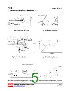
Switching Characteristics
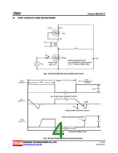
Turn-On Delay Time
tD (ON)
tR
tD(OFF)
tF
10
25
30
60
50
60
11
ns
ns
Rise Time
VDD =300V, ID =2.4A, RG=25Ω
(Note 1,2)
Turn-Off Delay Time
20
ns
Fall Time
25
ns
Total Gate Charge
QG
9.0
1.6
4.3
nC
nC
nC
VDS=480V, VGS=10V, ID=2.4A
Gate-Source Charge
QGS
QGD
(Note 1, 2)
Gate-Drain Charge
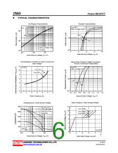
Drain-Source Diode Characteristics
Drain-Source Diode Forward Voltage
Continuous Drain-Source Current
Pulsed Drain-Source Current
Reverse Recovery Time
Reverse Recovery Charge
VSD
ISD
VGS = 0 V, ISD = 2.0 A
1.4
2.0
8.0
V
A
ISM
A
tRR
VGS = 0 V, ISD = 2.4A,
di/dt = 100 A/µs (Note1)
180
ns
µC
QRR
0.72
Note: 1. Pulse Test: Pulse Width ≤300µs, Duty Cycle≤2%
2. Essentially Independent of Operating Temperature
UNISONIC TECHNOLOGIES CO., LTD
3 of 8
QW-R502-053,E
www.unisonic.com.tw

 UTC [ Unisonic Technologies ]