uP0114
Application Information
1
2
3
4
FON#/ EN GND
8
7
6
5
VIN
GND
GND
GND
VOUT
VSET
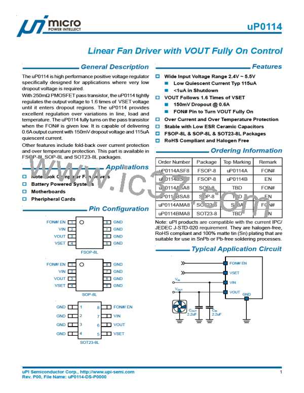
Figure 1. Recommended PCB Layout.
Layout Consideration
1. Place a local bypass capacitor as closed as possible
to the VIN pin. Use short and wide traces to minimize
parasitic resistance and inductance.
2. The GND pins should be soldered togher on ground
plane with maximum area and with multiple vias to inner
layer of ground place for improved thermal
performance.
uPI Semiconductor Corp., http://www.upi-semi.com
Rev. P00, File Name: uP0114-DS-P0000
9

 UNITPOWER [ ShenZhen XinDeYi Electronics Co., Ltd. ]