uP0114
Application Information
The uP0114 is high performance positive voltage regulator PD = (5V- 3.0V) x 0.2A = 0.4W
specifically designed for applications where very low
dropout voltage is required. It is capable of delivering 0.6A
output current with 150mV dropout voltage and 115uA
quiescent current.
This power dissipation is conducted through the package
into the ambient environment, and, in the process, the
temperature of the die (TJ) rises above ambient. Large
power dissipation may cause considerable temperature
raise in the regulator in large dropout applications. The
geometry of the package and of the printed circuit board
(PCB) greatly influence how quickly the heat is transferred
to the PCB and away from the chip. The most commonly
used thermal metrics for IC packages are thermal
resistance from the chip junction to the ambient air
surrounding the package (θJA):
Input/Output Capacitor Selection
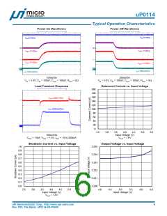
The uP0114 has a fast transient response that allows it to
handle large load changes associated with high current
applications. Proper selection of the output capacitor and
it’s ESR value determines stable operation and optimizes
performance. The typical application circuit shown in
Typical Application Circuit. The circuit was found to be
unconditionally stable with capacitor values from 2.2ìF to
47000ìF and ESR ranging from 0.5mΩ to greater then
75mΩ.
θJA = ( TJ -TA ) / PD
θJA specified in the Thermal Information section is
measured in the natural convection at TA = 25OC on a
Input capacitor: A minimum of 2.2uF ceramic capacitor high effective thermal conductivity test board (4 Layers,
is recommended to be placed directly next to the VIN pin. 2S2P) of JEDEC 51-7 thermal measurement standard.
This allows for the device being some distance from any The case point of θJC is on the pin 6 (GND) for FSOP-8
bulk capacitance on the rail.Additionally, bulk capacitance package.
may be added closely to the input supply pin of the uP0114
to ensure that VIN does not sag, improving load transient
response.
Given power dissipation PD, ambient temperature and
thermal resistance θJA, the junction temperature is
calculated as:
Output capacitor: Aminimum bulk capacitance of 2.2uF,
TJ = TA + ΔTJA = TA + PD x θJA
along with a 0.1uF ceramic decoupling capacitor is
To limit the junction temperature within its maximum rating,
recommended. Increasing the bulk capacitance will
the allowable maximum power dissipation is calculated
improve the overall transient response. The use of multiple
as:
lower value ceramic capacitors in parallel to achieve the
desired bulk capacitance will not cause stability issues.
Although designed for use with ceramic output capacitors,
the uP0114 is extremely tolerant of output capacitor ESR
values and thus will also work comfortably with tantalum
output capacitors.
PD(MAX) = ( TJ(MAX) -TA ) /θJA
where TJ(MAX) is the maximum operation junction
temperature 125OC, TA is the ambient temperature and
the θJA is the junction to ambient thermal resistance. θJA
of PSOP-8 packages is 75OC/W on JEDEC 51-7 (4 layers,
2S2P) thermal test board with minimum copper area. The
maximum power dissipation at TA = 25¢X C can be
calculated as:
Thermal Consideration
The uP0114 integrates internal thermal limiting function
to protect the device from damage during fault conditions.
However, continuously keeping the junction near the
thermal shutdown temperature may remain possibility to
affect device reliability. It is highly recommended to keep
the junction temperature below the recommended
operation condition 125OC for maximum reliability.
P
D(MAX) = (125OC - 25OC) / 75OC/W = 1.33W
The thermal resistance θJA highly depends on the PCB
design. Copper plane under the exposed pad is an
effective heatsink and is useful for improving thermal
conductivity.
Power dissipation in the device is calculated as:
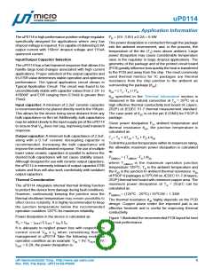
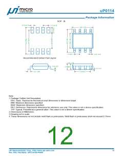
Figure 1 illustrated the recommended PCB layout for best
thermal performance.
ΠΔ = (ςΙΝ − ςΟΥΤ) ξ ΙΟΥΤ + ςΙΝ ξ ΙΘ
It is adequate to neglect power loss with respective to
control circuit VIN x IQ when considering thermal
management in uP0114 Take the following moderate
operation condition as an example: VIN = 5V, VOUT = 3V,
IOUT = 0.2A, the power dissipation is:
uPI Semiconductor Corp., http://www.upi-semi.com
Rev. P00, File Name: uP0114-DS-P0000
8

 UNITPOWER [ ShenZhen XinDeYi Electronics Co., Ltd. ]