UCD9090
SLVSA30A –APRIL 2011–REVISED AUGUST 2011
www.ti.com
Table 11. Configuration Options
Data Flash via JTAG
Data Flash via I2C
PMBus Commands via I2C
Data Flash Export (.srec or hex
type file)
Data Flash Export (.svf type file)
Dedicated programmer
Project file I2C/PMBus script
Off-Board Configuration
On-Board Configuration
Fusion tools (with exclusive bus
access via USB to I2C adapter)
Fusion tools (with exclusive bus
access via USB to I2C adapter)
Data flash export
IC
Fusion tools (with exclusive bus
access via USB to I2C adapter)
Fusion tools (with exclusive bus
access via USB to I2C adapter)
The advantages of off-board configuration include:
•
•
•
Does not require access to device I2C bus on board.
Once soldered on board, full board power is available without further configuration.
Can be partially reconfigured once the device is mounted.
Full Configuration Update while in Normal Mode
Although performing a full configuration of the UCD9090 in a controlled test setup is recommended, there may be
times in which it is required to update the configuration while the device is in an operating system. Updating the
full configuration based on methods listed in DEVICE CONFIGURATION AND PROGRAMMING section while
the device is in an operating system can be challenging because these methods do not permit the UCD9090 to
operate as required by application during the programming. During described methods the GPIOs may not be in
the desired states which can disable rails that provide power to the UCD9090. To overcome this, the UCD9090
has the capability to allow full configuration update while still operating in normal mode.
Updating the full configuration while in normal mode will consist of disabling data flash write protection, erasing
the data flash, writing the data flash image and reset the device. It is not required to reset the device immediately
but make note that the UCD9090 will continue to operate based on previous configuration with fault logging
disabled until reset. See Configuration Programming of UCD Devices, available from the Documentation & Help
Center that can be selected from the Fusion GUI Help menu, for details.
JTAG INTERFACE
The JTAG port can be used for production programming. Four of the six JTAG pins can also be used as GPIOs
during normal operation. See the Pin Functions table at the beginning of the document and Table 4 for a list of
the JTAG signals and which can be used as GPIOs. The JTAG port is compatible with the IEEE Standard
1149.1-1990, IEEE Standard Test-Access Port and Boundary Scan Architecture specification. Boundary scan is
not supported on this device. The UCD9090 runs at 10% slower frequency while the JTAG is enabled to ensure
best JTAG operation.
The JTAG interface can provide an alternate interface for programming the device. It is disabled by default in
order to enable the GPIO pins with which it is multiplexed. There are two conditions under which the JTAG
interface is enabled:
1. On power-up if the data flash is blank, allowing JTAG to be used for writing the configuration parameters to a
programmed device with no PMBus interaction
2. When address 126 (0x7E) is detected at power up. A short to ground or an open condition on either address
pin will cause an address 126 (0x7E) to be generated which enables JTAG mode.
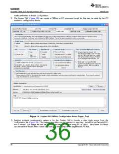
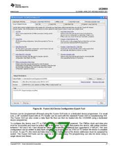
The Fusion GUI can create SVF files (See DEVICE CONFIGURATION AND PROGRAMMING section) based on
a given data flash configuration which can be used to program the desired configuration by JTAG. For Boundary
Scan Description Language (BSDL) file that supports the UCD9090 see the product folder in www.ti.com.
INTERNAL FAULT MANAGEMENT AND MEMORY ERROR CORRECTION (ECC)
The UCD9090 verifies the firmware checksum at each power up. If it does not match, then the device waits for
I2C commands but does not execute the firmware. A device configuration checksum verification is also
performed at power up. If it does not match, the factory default configuration is loaded. The PMBALERT# pin is
asserted and a flag is set in the status register. The error-log checksum validates the contents of the error log to
make sure that section of flash is not corrupted.
38
Copyright © 2011, Texas Instruments Incorporated

 TI [ TEXAS INSTRUMENTS ]