UCD9090
www.ti.com
SLVSA30A –APRIL 2011–REVISED AUGUST 2011
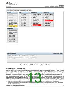
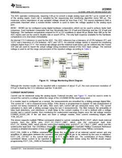
The ADC operates continuously, requiring 3.89 μs to convert a single analog input and 46.7 μs to convert all 12
of the analog inputs. Each rail is sampled by the sequencing and monitoring algorithm every 400 μs. The
maximum source impedance of any sampled voltage should be less than 4 kΩ. The source impedance limit is
particularly important when a resistor-divider network is used to lower the voltage applied to the analog input
pins.
MON1 - MON6 can be configured using digital hardware comparators, which can be used to achieve faster fault
responses. Each hardware comparator has four thresholds (two UV (Fault and Warning) and two OV (Fault and
Warning)). The hardware comparators respond to UV or OV conditions in about 80 μs (faster than 400 µs for the
ADC inputs) and can be used to disable rails or assert GPOs. The only fault response available for the hardware
comparators is to shut down immediately.
An internal 2.5-V reference is used by the ADC. The ADC reference has a tolerance of ±0.5% between 0°C and
125°C and a tolerance of ±1% between –40°C and 125°C. An external voltage divider is required for monitoring
voltages higher than 2.5 V. The nominal rail voltage and the external scale factor can be entered into the Fusion
GUI and are used to report the actual voltage being monitored instead of the ADC input voltage. The nominal
voltage is used to set the range and precision of the reported voltage according to Table 3.
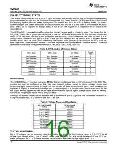
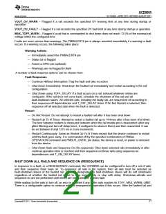
MON1 – MON6
Fast Digital
Comparators
MON1
12-bit
SAR ADC
200ksps
M
U
X
MON2
.
.
.
.
MON13
Analog
Inputs
(12)
Glitch
Filter
MON1 – MON13
Internal
2.5Vref
0.5%
Figure 10. Voltage Monitoring Block Diagram
Although the monitor results can be reported with a resolution of about 15 μV, the real conversion resolution of
610 μV is fixed by the 2.5-V reference and the 12-bit ADC.
CURRENT MONITORING
Current can be monitored using the analog inputs. External circuitry, see Figure 11, must be used in order to
convert the current to a voltage within the range of the UCD9090 MONx input being used.
If a monitor input is configured as a current, the measurements are smoothed by a sliding-average digital filter.
The current for 1 rail is measured every 200μs. If the device is programmed to support 10 rails (independent of
current not being monitored at all rails), then each rail's current will get measured every 2ms. The current
calculation is done with a sliding average using the last 4 measurements. The filter reduces the probability of
false fault detections, and introduces a small delay to the current reading. If a rail is defined with a voltage
monitor and a current monitor, then monitoring for undercurrent warnings begins once the rail voltage reaches
POWER_GOOD_ON. If the rail does not have a voltage monitor, then current monitoring begins after
TON_DELAY.
The device supports multiple PMBus commands related to current, including READ_IOUT, which reads external
currents from the MON pins; IOUT_OC_FAULT_LIMIT, which sets the overcurrent fault limit;
IOUT_OC_WARN_LIMIT, which sets the overcurrent warning limit; and IOUT_UC_FAULT_LIMIT, which sets the
undercurrent fault limit. The UCD90xxx Sequencer and System Health Controller PMBus Command Reference
contains a detailed description of how current fault responses are implemented using PMBus commands.
IOUT_CAL_GAIN is a PMBus command that allows the scale factor of an external current sensor and any
amplifiers or attenuators between the current sensor and the MON pin to be entered by the user in milliohms.
IOUT_CAL_OFFSET is the current that results in 0 V at the MON pin. The combination of these PMBus
commands allows current to be reported in amperes. The example below using the INA196 would require
programming IOUT_CAL_GAIN to Rsense(mΩ)×20.
Copyright © 2011, Texas Instruments Incorporated
17

 TI [ TEXAS INSTRUMENTS ]