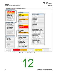
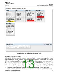
UCD9090
SLVSA30A –APRIL 2011–REVISED AUGUST 2011
www.ti.com
PIN SELECTED RAIL STATES
This feature allows with the use of up to 3 GPIs to enable and disable any rail. This is useful for implementing
system low-power modes and the Advanced Configuration and Power Interface (ACPI) specification that is used
for operating system directed power management in servers and PCs. In up to 8 system states, the power
system designer can define which rails are on and which rails are off. If a new state is presented on the input
pins, and a rail is required to change state, it will do so with regard to its sequence-on or sequence-off
dependencies.
The OPERATION command is modified when this function causes a rail to change its state. This means that the
ON_OFF_CONFIG for a given rail must be set to use the OPERATION command for this function to have any
effect on the rail state. The first 3 pins configured with the GPI_CONFIG command are used to select 1 of 8
system states. Whenever the device is reset, these pins are sampled and the system state, if enabled, will be
used to update each rail state. When selecting a new system state, changes to the status of the GPIs must not
take longer than 1 microsecond. See the UCD90xxx Sequencer and System Health Controller PMBus Command
Reference for complete configuration settings of PIN_SELECTED_RAIL_STATES.
Table 2. GPI Selection of System States
System
State
GPI 2 State
GPI 1 State
GPI 0 State
NOT Asserted
NOT Asserted
NOT Asserted
NOT Asserted
Asserted
NOT Asserted
NOT Asserted
Asserted
NOT Asserted
Asserted
0
1
2
3
4
5
6
7
NOT Asserted
Asserted
Asserted
NOT Asserted
NOT Asserted
Asserted
NOT Asserted
Asserted
Asserted
Asserted
NOT Asserted
Asserted
Asserted
Asserted
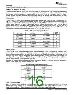
MONITORING
The UCD9090 has 11 monitor input pins (MONx) that are multiplexed into a 2.5V referenced 12-bit ADC. The
monitor pins can be configured so that they can measure voltage signals to report voltage, current and
temperature type measurements. A single rail can include all three measurement types, each monitored on
separate MON pins. If a rail has both voltage and current assigned to it, then the user can calculate power for the
rail. Digital filtering applied to each MON input depends on the type of signal. Voltage inputs have no filtering.
Current and temperature inputs have a low-pass filter.
Although the monitor results can be reported with a resolution of about 15 μV, the real conversion resolution of
610 μV is fixed by the 2.5-V reference and the 12-bit ADC.
Table 3. Voltage Range and Resolution
VOLTAGE RANGE
(Volts)
RESOLUTION
(millivolts)
0 to 127.99609
0 to 63.99805
0 to 31.99902
0 to 15.99951
0 to 7.99976
0 to 3.99988
0 to 1.99994
0 to 0.99997
3.90625
1.95313
0.97656
0.48824
0.24414
0.12207
0.06104
0.03052
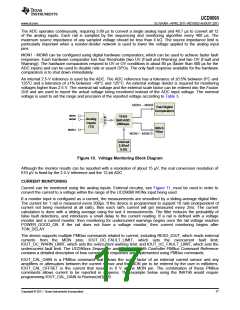
VOLTAGE MONITORING
Up to 12 voltages can be monitored using the analog input pins. The input voltage range is 0 V–2.5 V for all
MONx inputs except MON11 (pin 37) which has a range of 0.2V–2.5V. Any voltage between 0 V and 0.2 V on
these pins is read as 0.2 V. External resistors can be used to attenuate voltages higher than 2.5 V.
16
Copyright © 2011, Texas Instruments Incorporated

 TI [ TEXAS INSTRUMENTS ]