UCD90320
ZHCSFI3B –AUGUST 2016–REVISED MAY 2019
www.ti.com.cn
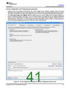
Device Configuration and Programming (continued)
The UCD90320 must be powered when it is being programmed via the PMBus or I2C interface. The PMBus
clock and data pins must be accessible and must be pulled high to the same V33D supply that powers the
device, with pullup resistors between 1 kΩ and 2 kΩ. Do not introduce additional bus capacitance less than 100
pF. When programming multiple UCD90320 devices over I2C, programming must be done individually.
Specifically, the clock and data lines must be multiplexed such that only one device is written by the programmer
at a time.
To update the device configuration in an operating system, the PMBus command method can be used to update
thresholds, timeout periods, and dependencies while the system is operating. Because the new configuration is
written into RAM, it takes effect immediately. However, pin-function-related configurations (change of rails,
change of GPI/GPO functions for example) may not work correctly until after a device reset. This delay may
indicate a problem in an operating system. For example, undesired states in the GPI, GPO, or RESET pin may
disable rails that provide power to the UCD90320, and thus terminate the programming process before it is
completed. Using the data flash image method can overcomes this problem by directly writing new configuration
into the data flash. This method allows a full configuration while the system is operating. It is not required to reset
the device immediately but the UCD90320 continues to operate based on previous configuration until a device
reset.
The JTAG port is compatible with IEEE Standard 1149.1-1990, Test-Access Port and Boundary Scan
Architecture specification. The UCD90320 device supports boundary scan. The UCD90320 device supports does
not support configuration programming via JTAG.
42
Copyright © 2016–2019, Texas Instruments Incorporated

 TI [ TEXAS INSTRUMENTS ]