UCD90320
www.ti.com.cn
ZHCSFI3B –AUGUST 2016–REVISED MAY 2019
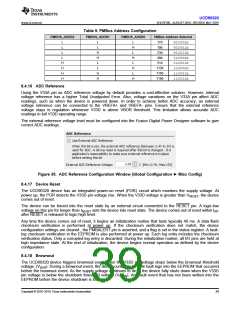
Table 5. PMBus Address Configuration
PMBUS_ADDR2
PMBUS_ADDR1
PMBUS_ADDR0
PMBus Address Selected
L
L
L
L
L
H
L
17d
19d
0010001b
0010011b
0010111b
0110001b
0110011b
1110001b
1110011b
1110111b
L
H
H
L
23d
L
H
L
49d
H
H
H
H
51d
L
H
L
113d
115d
119d
H
H
H
8.4.16 ADC Reference
Using the V33A pin as ADC reference voltage by default provides a cost-effective solution. However, internal
voltage reference has a higher Total Unadjusted Error. Also, voltage variations on the V33A pin affect ADC
readings, such as when the device is powered down. In order to achieve better ADC accuracy, an external
voltage reference can be connected to the VREFA+ and VREFA- pins. Ensure that the external reference
voltage stays in regulation whenever V33D is above VBOR threshold. This limitation allows accurate ADC
readings in full V33D operating range.
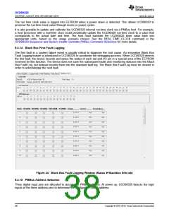
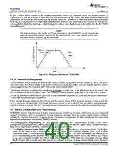
The external reference voltage level must be configured into the Fusion Digital Power Designer software to give
correct ADC readings.
Figure 35. ADC Reference Configuration Window (Global Configuration ► Misc Config)
8.4.17 Device Reset
The UCD90320 device has an integrated power-on reset (POR) circuit which monitors the supply voltage. At
power up, the POR detects the V33D pin voltage rise. When the V33D voltage is greater than VRESET, the device
comes out of reset.
The device can be forced into the reset state by an external circuit connected to the RESET
voltage on this pin for longer than tRESET sets the device into reset state. The device comes out of reset within tIRT
after RESET is released to logic-high level.
̅
pin. A logic-low
̅
Any time the device comes out of reset, it begins an initialization routine that lasts typically 40 ms. A data flash
checksum verification is performed at power up. If the checksum verification does not match, the device
configuration settings are cleared , the PMBALERT pin is asserted, and a flag is set in the status register. A fault-
log checksum verification in the EEPROM is also performed at power up. Each log entry includes the checksum
verification status. Only a corrupted log entry is discarded. During the initialization routine, all I/O pins are held at
high impedance state. At the end of initialization, the device begins normal operation as defined by the device
configuration.
8.4.18 Brownout
The UCD90320 device triggers brownout event when the V33D pin voltage drops below the brownout threshold
voltage, (VBOR). During a brownout event, the device continues to write fault logs into the EEPROM that occurred
before the brownout event. As the supply voltage continues to drop, the device fully shuts down when the V33D
pin voltage is below the shutdown threshold voltage (VSHDN). Any fault event that has not been written into the
EEPROM before the device shutdown is lost.
Copyright © 2016–2019, Texas Instruments Incorporated
39

 TI [ TEXAS INSTRUMENTS ]