UCD90320
ZHCSFI3B –AUGUST 2016–REVISED MAY 2019
www.ti.com.cn
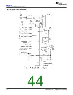
Typical Application (continued)
7. Margining configuration
8. Other configurations including but not limited to
–
–
–
–
–
Pin Selected Rail States
Watchdog Timer
System Reset
Sync Clock
Fault Pins
Click Write to Hardware to apply the changes. In online mode, the then click Store RAM to Flash to
permanently store the new configuration into the data flash of the device.
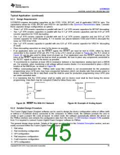
9.2.3 Application Curves
PMBus control pin de-assertion
Rail 1 EN with 5-ms turn-off delay
PMBus control pin assertion
Rail 1 EN with 5-ms turn-on delay
Rail 2 EN with 10-ms turn-off delay
Rail 2 EN with 10-ms turn-on delay
Rail 3 EN with 15-ms turn-off delay
Rail 3 EN with 15-ms turn-on delay
Time
Time
Figure 42. Shut-Down Waveforms
Figure 41. Start-Up Waveforms
10 Power Supply Recommendations
Power the UCD90320 device from a 3.3-V power supply.
If internal reference is used, V33A acts as ADC reference and is assumed to be exactly 3.3 V. Any input voltage
deviation from 3.3 V introduces an error to ADC reference and to the ADC results. Therefore, the 3.3-V power
supply must be tightly regulated and allow only a very small voltage fluctuation (including voltage ripple and
voltage deviation caused by load transients).
If external reference is used, the 3.3-V power supply needs to meet only the minimum requirements specified in
the Recommended Operating Conditions table and the Electrical Characteristics table.
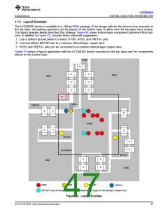
11 Layout
11.1 Layout Guidelines
•
•
•
Place the decoupling capacitors as close as possible to the device.
Connect the BPCAP decoupling capacitors as close as possible to pin D6.
MARGIN pins output PWM signals that have fast-edges. Route these signals away from sensitive analog
signals. It is a good practice to place resistor R4 and capacitor C1 (as shown in Figure 22) as close as
possible to the MARGIN pin, minimizing the propagation distance of the fast-edge PWM signals on the PCB.
•
Resistor R3 can be placed near the power supply feedback node to isolate the feedback node from noise
sources on the PCB. If resistor R4 and capacitor C1 cannot be located close to the MARGIN pin, add a
termination resistor in series with a value between 20-Ω and 33-Ω. Locate it near the MARGIN pin.
46
Copyright © 2016–2019, Texas Instruments Incorporated

 TI [ TEXAS INSTRUMENTS ]