UCD90320
www.ti.com.cn
ZHCSFI3B –AUGUST 2016–REVISED MAY 2019
Typical Application (continued)
9.2.1 Design Requirements
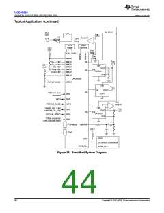
UCD90320 requires decoupling capacitors on the V33D, V33A, BPCAP, and (if applicable) VREFA+ pins. The
capacitance values for V33A, BPCAP and VREFA+ are specified in the Electrical Characteristics table. Consider
these capacitor design configurations as options.
•
•
Three 1-μF X7R ceramic capacitors in parallel with two 0.1-μF X7R ceramic capacitors for BPCAP decoupling
Two 1-μF X7R ceramic capacitors in parallel with four 0.1-μF X7R ceramic capacitors and two 0.01-μF X7R
ceramic capacitors for V33D decoupling
•
•
One 1-μF X7R ceramic capacitor in parallel with one 0.1-μF X7R ceramic capacitor and one 0.01-μF X7R
ceramic capacitor for V33A decoupling. A 1-Ω resistor can placed between V33D and V33A to decouple the
noise on V33D from V33A.
One 1-μF X7R ceramic capacitor in parallel with one 0.01-μF X7R ceramic capacitor for VREFA+ decoupling
(if used)
•
•
Place decoupling capacitors as close to the device as possible.
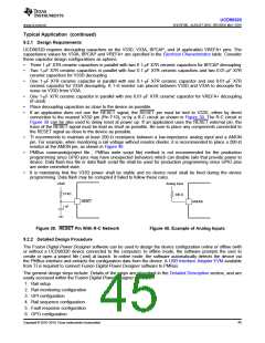
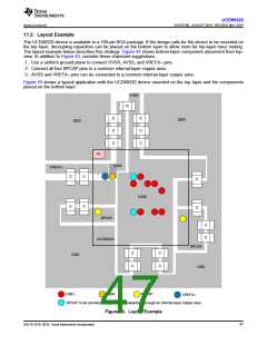
If an application does not use the RESET signal, the RESET pin must be tied to V33D, either by direct
connection to the nearest V33D pin (Pin F10), or by a R-C circuit as shown in Figure 39. The R-C circuit in
Figure 39 can be also used to delay reset at power up. If an application uses the RESET external pin, the
trace of the RESET signal must be kept as short as possible. Be sure to place any components connected to
the RESET signal as close to the device as possible.
•
•
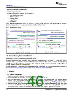
TI recommends to maintain at least 200-Ω resistance between a low-impedance analog input and a AMON
pin. For example, when monitoring a rail voltage without resistor divider, it is recommended to place a 200-Ω
resistor at the AMON pin, as shown in Figure 40.
PMBus commands(project file , PMBus write script file) method is not recommended for the production
programming since GPIO pins may have unexpected behaviors which can disable rails that provide power to
device. Data flash hex file or data flash script file shall be used for production programming since GPIO pins
are under controlled state.
•
It is mandatory that the V33D power shall be stable and no device reset shall be fired during the device
programming. Data flash may be corrupted if failed to follow these rules.
V33D
Analog Input
10 kΩ
200 Ω
RESET
AMONx
1 nF
Figure 39. RESET Pin With R-C Network
9.2.2 Detailed Design Procedure
Figure 40. Example of Analog Inputs
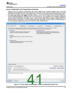
The Fusion Digital Power Designer software can be used to design the device configuration online or offline (with
or without a UCD90320 device connected to the computer). In offline mode, the software prompts the user to
create or open a project file (.xml) at launch. In online mode, the software automatically detects the device via
the PMBus interface and extracts the configuration data from the device. A USB Interface Adapter EVM available
from TI is required to connect Fusion Digital Power Designer software to PMBus.
The general design steps include. Details of the steps are described in the Detailed Description section, and are
easily accessed within the Fusion Digital Power Designer software .
1. Rail setup
2. Rail monitoring configuration
3. GPI configuration
4. Rail sequence configuration
5. Fault response configuration
6. GPO configuration
Copyright © 2016–2019, Texas Instruments Incorporated
45

 TI [ TEXAS INSTRUMENTS ]