UCC28610
www.ti.com ......................................................................................................................................... SLUS888C–JANUARY 2009–REVISED SEPTEMBER 2009
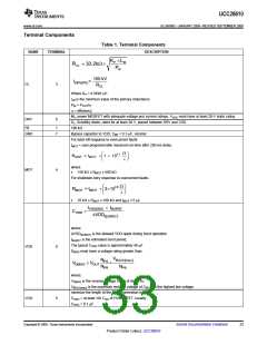
Terminal Components
Table 1. Terminal Components
NAME
TERMINAL
DESCRIPTION
KP ´LM
RCL = 33.2kW ´
P
IN
100 kV
IDRV(PK)
=
CL
3
RCL
Where KP = 0.54W/ µH
LM is the minimum value of the primary inductance
PIN = POUT/η
η = efficiency
M1, power MOSFET with adequate voltage and current ratings, VVGS must have at least 20-V static rating.
D1, Schottky diode, rated for at least 30 V, placed between DRV and VDD
100 kΩ
DRV
6
FB
1
7
GND
Bypass capacitor to VDD, CBP = 0.1-µF, ceramic
For latch-off response to overcurrent faults:
tMOT = user programmable maximum on-time after 250-ms delay.
W
æ
ç
è
ö
÷
ø
RMOT = tMOT ´ 1 ´ 1011
s
where
MOT
4
•
150 kΩ ≤ RMOT ≤ 500 kΩ
For shutdown-retry response to overcurrent faults:
W
æ
ç
è
ö
÷
ø
RMOT = tMOT ´ 2´1010
s
•
25 kΩ ≤ RMOT ≤ 100 kΩ and tMOT ≤ 5 µs
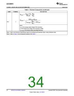
IVDD(GM) ´ tBURST
CVDD
=
DVDD BURST
(
)
where:
ΔVDD(BURST) is the allowed VDD ripple during burst operation
tBURST is the estimated burst period,
The typical CVDD value is approximately 48 µF
DBIAS must have a voltage rating greater than:
VDD
8
VBULK max
NPS
NPB
(
)
VDBIAS ³ VOUT
+
NPB
where:
VDBIAS is the reverse voltage rating of diode D2
VBULK(max) is the maximum rectified voltage of CBULK at the highest line voltage
minimize the length of the CVGG connection to GND
CVGG = at least 10x CGS of HVMOSFET, usually
CVGG = 0.1 µF.
VGG
5
Copyright © 2009, Texas Instruments Incorporated
Submit Documentation Feedback
33
Product Folder Link(s): UCC28610

 TI [ TEXAS INSTRUMENTS ]