UCC28951
www.ti.com.cn
ZHCSIQ7A –AUGUST 2018 –REVISED DECEMBER 2021
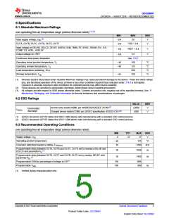
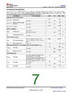
VDD = 12 V, TA = TJ = –40°C to +125°C, CVDD = 1 µF, CREF = 1 µF, RAB = 22.6 kΩ, RCD = 22.6 kΩ, REF = 13.3 kΩ, RSUM
=
124 kΩ, RTMIN = 88.7 kΩ, RT = 59 kΩconnected between RT pin and 5-V voltage supply to set FSW = 100 kHz (FOSC = 200
kHz) (unless otherwise noted). All component designations are from 图8-3.
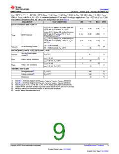
PARAMETER
TEST CONDITIONS
MIN
TYP
MAX
UNIT
LIGHT-LOAD EFFICIENCY CIRCUIT
VDCM = 0.4 V, Sweep CS confirm there are
OUTE and OUTF pulses, TA = 25°C
0.37
0.39
0.39
0.41
V
V
VDCM = 0.4 V, Sweep CS, confirm there are
OUTE and OUTF pulses, 0°C ≤TA ≤
85°CDCM threshold, (6)
0.364
0.416
VDCM
DCM threshold
VDCM = 0.4 V, Sweep CS, confirm there are
OUTE and OUTF pulses, –40°C ≤TA ≤
125°C(6)
0.35
14
0.39
0.43
26
V
CS < DCM threshold
IDCM_SRC
DCM Sourcing Current
µA
CS < DCM threshold, TA = 25°C
20
OUTPUTS OUTA, OUTB, OUTC, OUTD, OUTE, OUTF
Sink and source peak
ISINK/SRC
TA = 25°C
0.2
A
current(6)
IOUT = 20 mA
10
5
35
30
RSRC
Output source resistance
Ω
IOUT = 20 mA, TA = 25°C
IOUT = 20 mA
20
10
RSINK
Output sink resistance
Ω
IOUT = 20 mA, TA = 25°C
THERMAL SHUTDOWN
Rising threshold(6)
TA = 25°C
TA = 25°C
160
140
20
°C
°C
°C
Falling threshold(6)
Hysteresis
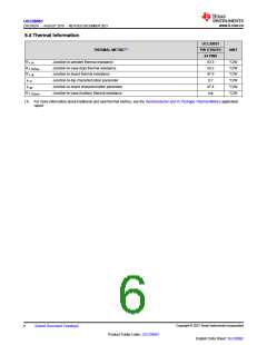
(1) See 图7-1 for timing diagram and TABSET1, TABSET2, TCDSET1, TCDSET2 definitions.
(2) See 图7-4 for timing diagram and TAFSET1, TAFSET2, TBESET1, TBESET2 definitions.
(3) Pair of outputs OUTC, OUTE and OUTD, OUTF always going high simultaneously.
(4) Outputs A or B are never allowed to go high if both outputs OUTE and OUTF are high.
(5) All delay settings are measured relative to 50% of pulse amplitude.
(6) Verified during characterization only.
Copyright © 2023 Texas Instruments Incorporated
Submit Document Feedback
9
Product Folder Links: UCC28951
English Data Sheet: SLUSDB2

 TI [ TEXAS INSTRUMENTS ]