UCC28951
www.ti.com.cn
ZHCSIQ7A –AUGUST 2018 –REVISED DECEMBER 2021
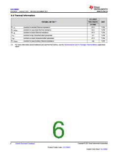
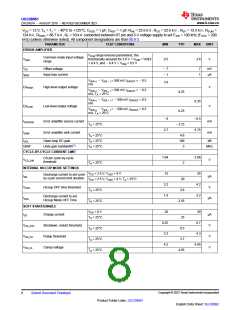
6 Specifications
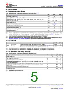
6.1 Absolute Maximum Ratings
over operating free-air temperature range (unless otherwise noted) (1) (2)
MIN
–0.4
–0.4
MAX
20
UNIT
V
(3)
Input supply voltage, VDD
OUTA, OUTB, OUTC, OUTD, OUTE, OUTF
VDD + 0.4
V
Input voltage on DELAB, DELCD, DELEF, SS/EN, DCM, TMIN, RT, SYNC, RSUM, EA+, EA-,
COMP, CS, ADEL, ADELEF
VREF + 0.4
5.6
V
V
–0.4
–0.4
Output voltage on VREF
Continuous total power dissipation
Operating virtual junction temperature, TJ
Operating ambient temperature, TA
Lead temperature (soldering, 10 s)
Storage temperature, Tstg
See 节6.7
150
°C
°C
°C
°C
–40
–40
125
300
150
–65
(1) Stresses beyond those listed under Absolute Maximum Ratings may cause permanent damage to the device. These are stress ratings
only, and functional operation of the device at these or any other conditions beyond those indicated under 节6.3 is not implied.
Exposure to absolute-maximum-rated conditions for extended periods may affect device reliability.
(2) These devices are sensitive to electrostatic discharge; follow proper device handling procedures.
(3) All voltages are with respect to GND unless otherwise noted. Currents are positive into, negative out of the specified terminal. See 节
Mechanical, Packaging, and Orderable Information for thermal limitations and considerations of packages.
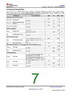
6.2 ESD Ratings
VALUE
±2000
±500
UNIT
V
Human body model (HBM), per ANSI/ESDA/JEDEC JS-001(1)
Electrostatic
discharge
V(ESD)
Charged device model (CDM), per JEDEC specification JESD22-C101(2)
V
(1) JEDEC document JEP155 states that 500-V HBM allows safe manufacturing with a standard ESD control process.
(2) JEDEC document JEP157 states that 250-V CDM allows safe manufacturing with a standard ESD control process.
6.3 Recommended Operating Conditions
over operating free-air temperature range (unless otherwise noted)
MIN
8
TYP
MAX
17
UNIT
V
Supply voltage, VDD
12
Operating junction temperature
125
1000
°C
–40
50
Converter switching frequency setting, FSW(nom)
Programmable delay between OUTA, OUTB and OUTC, OUTD set by resistors DELAB and
kHz
30
30
1000
1400
ns
ns
(1)
DELCD and parameter KA
Programmable delay between OUTA, OUTF and OUTB, OUTE set by resistor DELEF, and
(1)
parameter KEF
Programmable DCM as percentage of voltage at CS(1)
5%
30%
800
Programmable TMIN
100
ns
(1) Verified during characterization only.
Copyright © 2023 Texas Instruments Incorporated
Submit Document Feedback
5
Product Folder Links: UCC28951
English Data Sheet: SLUSDB2

 TI [ TEXAS INSTRUMENTS ]