UCC28951
www.ti.com.cn
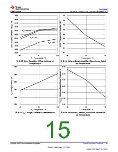
ZHCSIQ7A –AUGUST 2018 –REVISED DECEMBER 2021
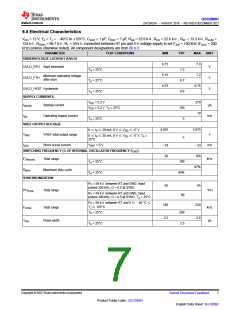
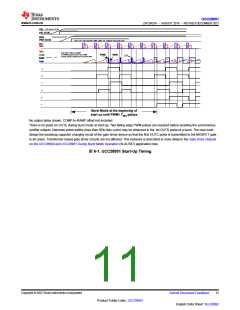
7.3-V rise, 6.7-V fall
VDD
VDD_GOOD
4.8-V rise, 4.6-V fall
VREF
VREF_GOOD
SS > 0.5 V, then release COMP, DCM, CS , Outputs A,B,C,D,E and F
CLK
TMIN
TMIN
Add 0.85 V offset to RAMP
No PWM pulses shorter than TMIN
except during cycle-by-cycle current limit
PWM
TMIN
COMP
RAMP
PWM
2 VP-P
A
B
C
D
E
F
Burst Mode at the beginning of
start up until PWM> TMIN pulses
No output delay shown, COMP-to-RAMP offset not included.
There is no pulse on OUTE during burst mode at start-up. Two falling edge PWM pulses are required before enabling the synchronous
rectifier outputs. Narrower pulse widths (less than 50% duty cycle) may be observed in the 1st OUTD pulse of a burst. The user must
design the bootstrap capacitor charging circuit of the gate driver device so that the first OUTC pulse is transmitted to the MOSFET gate
in all cases. Transformer based gate driver circuits are not affected. This behavior is described in more detail in the Gate Drive Outputs
on the UCC28950 and UCC28951 During Burst Mode Operation (SLAU787) application note.
图6-1. UCC28951 Start-Up Timing
Copyright © 2023 Texas Instruments Incorporated
Submit Document Feedback
11
Product Folder Links: UCC28951
English Data Sheet: SLUSDB2

 TI [ TEXAS INSTRUMENTS ]