UCC28951
www.ti.com.cn
ZHCSIQ7A –AUGUST 2018 –REVISED DECEMBER 2021
8.2.3 Application Curves
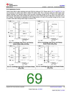
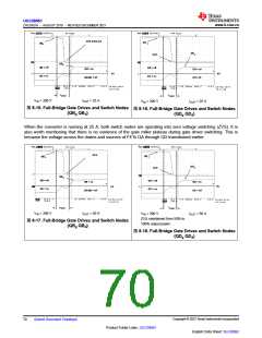
Switch node QBd is valley switching and node QDd has achieved ZVS. Please refer to 图 8-13 and 图 8-14. It is
not uncommon for switch node QDd to obtain ZVS before QBd. This is because during the QDd switch node
voltage transition, the reflected output current provides immediate energy for the LC tank at the switch node.
Where at the QBd switch node transition the primary has been shorted out by the high-side or low-side FETs in
the H bridge. This transition is dependent on the energy stored in LS and LLK to provide energy for the LC tank
at switch node QBd making it take longer to achieve ZVS.
Valley Switching
QB
QD
d
d
Valley Switching
QD g
QBg
QB = off
QA= on
QD = on
QC = off
QD = off
QC = on
QB = on
0V
0V
QA/QB = off
tCDSET
tABSET
tD
Slight Delay after t
before Miller Plateau
tD
Slight Delay after t
before Miller Plateau
CDSET
ABSET
VIN = 390 V
IOUT = 5 A
VIN = 390 V
IOUT = 5 A
图8-12. Full-Bridge Gate Drives and Primary
图8-11. Full-Bridge Gate Drives and Primary
Switch Nodes (QDg QDd)
Switch Nodes (QBd and QDd)
Valley Switching
QB d
QD d
QDg
QBg
ZVS
0V
QD = off
QB = off
QD = on
QB = on
0V
0V
QC = on
QA = on
QC = off
QA/QB = off
tCDSET
tABSET
tD
tD
Slight Delay after t
Slight Delay after t
CDSET
ABSET
before Miller Plateau
before Miller Plateau
VIN = 390 V
IOUT = 10 A
VIN = 390 V
IOUT = 10 A
图8-14. Full-Bridge Gate Drives and Switch Nodes
图8-13. Full-Bridge Gate Drives and Switch Nodes
(QDg QDd)
(QBg QBd)
Copyright © 2023 Texas Instruments Incorporated
Submit Document Feedback
69
Product Folder Links: UCC28951
English Data Sheet: SLUSDB2

 TI [ TEXAS INSTRUMENTS ]