UCC28951
www.ti.com.cn
ZHCSIQ7A –AUGUST 2018 –REVISED DECEMBER 2021
10 Layout
10.1 Layout Guidelines
To increase the reliability and robustness of the design, TI recommends the following layout guidelines:
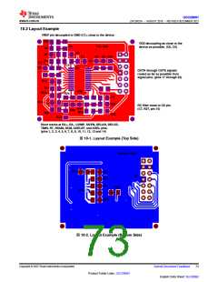
• For the VREF pin: decouple this pin to GND with a good quality ceramic capacitor. A 1-µF, X7R, 25-V
capacitor is recommended. Keep VREF PCB tracks as far away as possible from sources of switching noise.
• For the EA+ pin: this is the noninverting input to the error amplifier. It is a high impedance pin and is
susceptible to noise pickup. Keep tracks from this pin as short as possible.
• For theEA–pin: this is the inverting input to the error amplifier. It is a high impedance pin and is susceptible
to noise pickup. Keep tracks from this pin as short as possible.
• For theCOMP pin: the error amplifier compensation network is normally connected to this pin. Keep tracks
from this pin as short as possible.
• For theSS/EN pin: keep tracks from this pin as short as possible. If the Enable signal is coming from a remote
source then avoid running it close to any source of high dv/dt (MOSFET Drain connections for example) and
add a simple RC filter at the SS/EN pin.
• For the DELAB, DELCD, DELEF, TMIN, RT, RSUM, DCM, ADELEF and ADEL pins: the components
connected to these pins are used to set important operating parameters. Keep these components close to the
IC and provide short, low impedance return connections to the GND pin.
• For the CS pin: this connection is arguably the most important single connection in the entire PSU system.
Avoid running the CS signal traces near to sources of high dv/dt. Provide a simple RC filter as close to the pin
as possible to help filter out leading edge noise spikes which occur at the beginning of each switching cycle.
• For the SYNC pin: this pin is essentially a digital I/O port. If it is unused, then it may be left open circuit or tied
to ground through a 1-kΩresistor. If Synchronisation is used, then route the incoming Synchronisation signal
as far away from noise sensitive input pins as possible.
• For the OUTA, OUTB, OUTC, OUTD, OUTE and OUTF pins: these are the gate drive output pins. They have
a high dv/dt rate associated with their rising and falling edges. Keep the tracks from these pins as far away
from noise sensitive input pins as possible. Ensure that the return currents from these outputs do not cause
voltage changes in the analog ground connections to noise sensitive input pins. Follow the layout
recommendation for analog and power ground planes in 图7-18.
• For the VDD pin: this pin must be decoupled to GND using ceramic capacitors as detailed in the 节9 section.
Keep this capacitor as close to the VDD and GND pins as possible.
• For the GND pin: this pin provides the ground reference to the controller. Use a ground plane to minimize the
impedance of the ground connection and to reduce noise pickup.
Copyright © 2023 Texas Instruments Incorporated
English Data Sheet: SLUSDB2
72
Submit Document Feedback
Product Folder Links: UCC28951

 TI [ TEXAS INSTRUMENTS ]