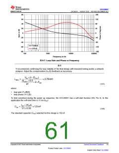
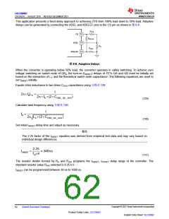
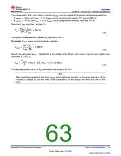
UCC28951
www.ti.com.cn
ZHCSIQ7A –AUGUST 2018 –REVISED DECEMBER 2021
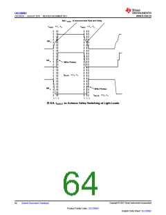
Initially, set the QC and QD turn-on delays (tCDSET) for the same delay as the QA and QB turn-on delays (Pin 6).
The following equations program the QC and QD turn-on delays (tCDSET) by properly selecting resistor RDELCD
(Pin 7).
tABSET = tCDSET
(135)
Resistor RCD programs tCDSET
:
TCDSET
RCD
=
´ 0.26 + CS´K ´1.3 » 30.6kW
A
(
)
5
(136)
The standard resistor RCD selected for this design is 30.1 kΩ.
备注
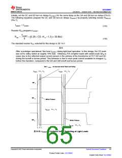
After a prototype operational, fine tune tCDSET during light-load operation. In this design, the CD node
was set to valley switch at roughly 10% load.. Obtaining ZVS at lighter loads with switch node QDd is
easier due to the reflected output current present in the primary of the transformer at FET QD and QC
during the turnoff or turnon period. This behavior is due to more peak current available to energize LS
before this transition, compared to the QA and QB turnoff and turnon period.
Set t
at resonant tank Peak and Valley
CDSET
tCDSET = t - t0
tCDSET = t - t3
1
4
QD
d
QC
g
Miller Plateau
tMILLER = t - t 1
2
QD g
Miller Plateau
tMILLER = t - t 4
5
t0 t1 t2
t3 t4 t5
图8-10. tCDSET to Achieve Valley Switching at Light Loads
Copyright © 2023 Texas Instruments Incorporated
Submit Document Feedback
65
Product Folder Links: UCC28951
English Data Sheet: SLUSDB2

 TI [ TEXAS INSTRUMENTS ]