UCC28951
www.ti.com.cn
ZHCSIQ7A –AUGUST 2018 –REVISED DECEMBER 2021
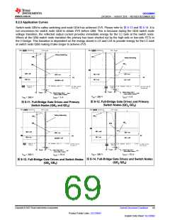
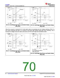
ZVS Achieved
QD
QBd
d
QDg
ZVS
QBg
QB = off
QD = off
QC = on
QB = on
QD = on
0V
0V
QA = on
QA/QB = off
QC= off
tABSET
tCDSET
VIN = 390 V
IOUT = 25 A
VIN = 390 V
IOUT = 25 A
图8-15. Full-Bridge Gate Drives and Switch Nodes
图8-16. Full-Bridge Gate Drives and Switch Nodes
(QBg QBd)
(QDg QDd)
When the converter is running at 25 A, both switch nodes are operating into zero voltage switching (ZVS). It is
also worth mentioning that there is no evidence of the gate miller plateau during gate driver switching. This is
because the voltage across the drains and sources of FETs QA through QD transitioned earlier.
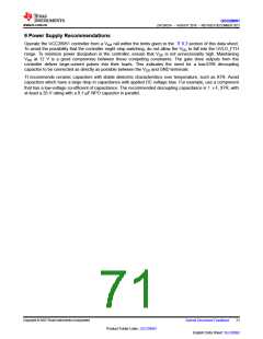
ZVS
QD d
QB d
QDg
ZVS
QBg
QB = off
QA = on
QD = off
QC = on
QB = on
QD = on
0V
0V
QA/QB = off
QC = off
tABSET
tCDSET
VIN = 390 V
IOUT = 50 A
VIN = 390 V
IOUT = 50 A
ZVS maintained from 50% to
100% output power
图8-17. Full-Bridge Gate Drives and Switch Nodes
(QBg QBd)
图8-18. Full-Bridge Gate Drives and Switch Nodes
(QDg QDd)
Copyright © 2023 Texas Instruments Incorporated
70
Submit Document Feedback
Product Folder Links: UCC28951
English Data Sheet: SLUSDB2

 TI [ TEXAS INSTRUMENTS ]