UCC28951
www.ti.com.cn
ZHCSIQ7A –AUGUST 2018 –REVISED DECEMBER 2021
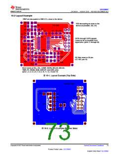
10.2 Layout Example
VREF pin decoupled to GND (C1), close to the device
R28
C8
VDD decoupling as close to the
device as possible. (C6, C5)
R6
Top Side
R2
R1
R7
C1
C6 C5 R15
R9
U1
C3
R5
C4
OUTA through OUTE signals
routed as far as possible from
signal pins. (pins 17 through 22)
R12
R11
R13
R16
R24
C7
R14
R27
R22
RC filter close to CS pin.
(C7, R27, pin 15)
R17
R26
R25
R28
R23
Short tracks at EA+, EA-, COMP, SS/EN, DELAB, DELCD,
TMIN, RT, RSUM, DCM, ADELEF, and ADEL pins.
(pins 1, 2, 3, 4, 5, 6, 7, 8, 9, 10, 11, 12, 13 and 14)
图10-1. Layout Example (Top Side)
Bottom Side
R29
C2
R3
R4
J1
R20
R8
R10
图10-2. Layout Example (Bottom Side)
Copyright © 2023 Texas Instruments Incorporated
Submit Document Feedback
73
Product Folder Links: UCC28951
English Data Sheet: SLUSDB2

 TI [ TEXAS INSTRUMENTS ]