UCC28951
www.ti.com.cn
ZHCSIQ7A –AUGUST 2018 –REVISED DECEMBER 2021
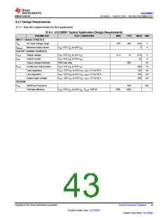
8.2.1 Design Requirements
表8-1 lists the requirements for this application.
表8-1. UCC28951 Typical Application Design Requirements
PARAMETER
TEST CONDITIONS
MIN
TYP
MAX
UNIT
INPUT CHARACTERISTICS
VIN
DC input voltage range
Maximum input current
370
390
410
2
V
A
IIN(max)
VIN= 370 VDC to 410 VDC
OUTPUT CHARACTERISTICS
VOUT
IOUT
Output voltage
VIN= 370 VDC to 410 VDC
11.4
12
12.6
50
V
Output current
VIN= 370 VDC to 410 VDC
A
Output voltage transient
Continuous output power
Load regulation
90% load step
600
mV
W
POUT
VIN= 370 VDC to 410 VDC
600
140
140
200
VIN = 370 VDC to 410 VDC, IOUT= 5 A to 50 A
VIN = 370 VDC to 410 VDC, IOUT= 5 A to 50 A
VIN = 370 VDC to 410 VDC, IOUT= 5 A to 50 A
mV
mV
mV
Line regulation
Output ripple voltage
SYSTEM
FSW
Switching Frequency
Full-load efficiency
100
kHz
VIN= 370 VDC to 410 VDC, POUT= 500 W
93%
94%
Copyright © 2023 Texas Instruments Incorporated
Submit Document Feedback
43
Product Folder Links: UCC28951
English Data Sheet: SLUSDB2

 TI [ TEXAS INSTRUMENTS ]