UCC28740
SLUSBF3A –JULY 2013–REVISED JULY 2013
www.ti.com
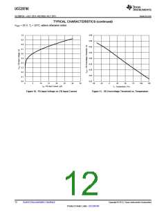
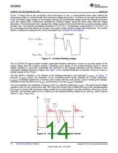
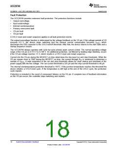
Figure 13 shows that as the secondary current decreases to zero, a clearly-defined down slope reflects the
decreasing rectifier VF combined with stray resistance voltage-drop (ISRS). To achieve an accurate representation
of the secondary output voltage on the auxiliary winding, the discriminator reliably blocks the leakage-inductance
reset and ringing while continuously sampling the auxiliary voltage during the down slope after the ringing
diminishes. The discriminator then captures the voltage signal at the moment that the secondary-winding current
reaches zero. The internal overvoltage threshold on VS is 4.6 V. Temperature compensation of –0.8 mV/°C on
the overvoltage threshold offsets the change in the output-rectifier forward voltage with temperature. The resistor
divider is selected as outlined in the VS pin description (see Detailed Pin Description).
Figure 13. Auxiliary-Winding Voltage
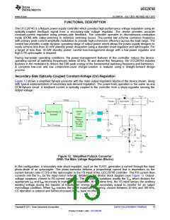
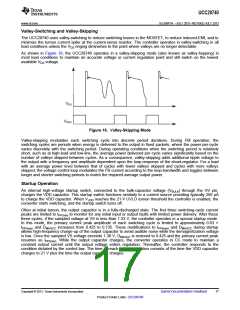
The UCC28740 VS-signal sampler includes signal-discrimination methods to ensure an accurate sample of the
output voltage from the auxiliary winding. Controlling some details of the auxiliary-winding signal to ensure
reliable operation is necessary; specifically, the reset time of the leakage inductance and the duration of any
subsequent leakage-inductance ringing. See Figure 14 for a detailed illustration of waveform criteria to ensure a
reliable sample on the VS pin.
The first detail to examine is the duration of the leakage-inductance reset pedestal, tLK_RESET, in Figure 14.
Because tLK_RESET mimics the waveform of the secondary-current decay, followed by a sharp downslope,
tLK_RESET is internally blanked for a duration which scales with the peak primary current. Keeping the leakage-
reset time to less than 600 ns for IPP(min), and less than 2.2 µs for IPP(max) is important.
The second detail is the amplitude of ringing on the VAUX waveform following tLK_RESET. The peak-to-peak voltage
variation at the VS pin must be less than 100 mVp-p for at least 200 ns before the end of the demagnetization
time (tDM). A concern with excessive ringing usually occurs during light or no-load conditions, when tDM is at the
minimum. The tolerable ripple on VS is scaled up to the auxiliary-winding voltage by RS1 and RS2, and is equal to
100 mV × (RS1 + RS2) / RS2
.
Figure 14. Auxiliary-Winding Waveform Details
14
Submit Documentation Feedback
Copyright © 2013, Texas Instruments Incorporated
Product Folder Links: UCC28740

 TI [ TEXAS INSTRUMENTS ]