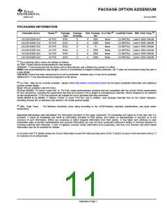
ꢀꢁꢁ ꢂ ꢃꢄ ꢅ ꢆꢇ ꢈ ꢆꢄ ꢈꢆꢂ ꢈ ꢆꢅ ꢈꢆ ꢉꢈ ꢆ ꢊꢆ ꢋ ꢄ
ꢌ ꢍ ꢎꢆꢏꢍ ꢎ ꢐꢑ ꢒꢓ ꢁꢔꢍ ꢕ ꢁꢀꢑ ꢑꢐꢖꢗꢆꢔꢍ ꢘ ꢐ ꢏ ꢎꢔ
ꢙ
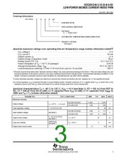
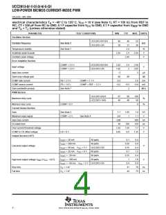
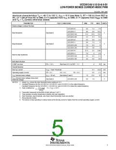
SGLS245 − MAY 2004
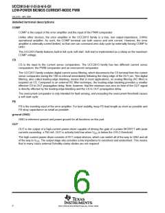
detailed descriptions (continued)
RC
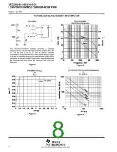
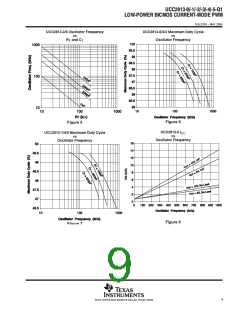
RC is the oscillator timing pin. For fixed frequency operation, set timing capacitor charging current by connecting
a resistor from REF to RC. Set frequency by connecting timing capacitor from RC to GND. For best perfomance,
keep the timing capacitor lead to GND as short and direct as possible. If possible, use separate ground traces
for the timing capacitor and all other functions.
The frequency of oscillation can be estimated with the following equations:
1.5
R C
UCC2813−0ń1ń2ń4 : F +
1.0
R C
UCC2813−3ńUCC2813−5 : F +
(1)
where frequency is in Hz, resistance is in ohms, and capacitance is in farads. The recommended range of the
timing resistors is between 10 kΩ and 200 kΩ and the timing capacitor is 100 pF to 1000 pF. Never use a timing
resistor less than 10 k.
To prevent noise problems, bypass V
An electrolytic capacitor may also be used in addition to the ceramic capacitor.
to GND with a ceramic capacitor as close to the V
pin as possible.
CC
CC
voltage reference (REF)
REF is the voltage reference for the error amplifier and also for many other functions on the IC. REF is also used
as the logic power supply for high-speed switching logic on the IC.
When V is greater than 1 V and less than the UVLO threshold, REF is pulled to ground through a 5-kΩ resistor.
CC
This means that REF can be used as a logic output indicating power system status. It is important for reference
stability that REF is bypassed to GND with a ceramic capacitor as close to the pin as possible. An electrolytic
capacitor may also be used in addition to the ceramic capacitor. A minimum of 0.1-µF ceramic capacitor is
required. Additional REF bypassing is required for external loads greater than 2.5 mA on the reference.
To prevent noise problems with high-speed switching transients, bypass REF to ground with a ceramic capacitor
close to the IC package.
power (V
)
CC
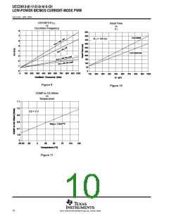
V
is the power input connection for this device. In normal operation, V
is powered through a current limiting
CC
CC
resistor. Although quiescent V
Total V
frequency and the MOSFET gate charge (Q ), average OUT current can be calculated from:
current is low, total supply current will be higher, depending on OUT current.
CC
current is the sum of quiescent V
current and the average OUT current. Knowing the operating
CC
CC
g
IOUT + Qg F.
(2)
7
POST OFFICE BOX 655303 • DALLAS, TEXAS 75265

 TI [ TEXAS INSTRUMENTS ]