ꢀꢁꢁ ꢂ ꢃꢄ ꢅ ꢆꢇ ꢈ ꢆꢄ ꢈꢆꢂ ꢈ ꢆꢅ ꢈꢆ ꢉꢈ ꢆ ꢊꢆ ꢋ ꢄ
ꢌ ꢍ ꢎꢆꢏꢍ ꢎ ꢐꢑ ꢒꢓ ꢁꢔꢍ ꢕ ꢁꢀꢑ ꢑꢐꢖꢗꢆꢔꢍ ꢘ ꢐ ꢏ ꢎꢔ
ꢙ
SGLS245 − MAY 2004
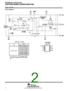
Ordering Information
813-
0
Q
UCC2
D
R
Q1
Q100 INDICATOR
TAPE and REEL INDICATOR
PACKAGE
D
= Plastic SOIC
AUTOMOTIVE TEMPERATURE RANGE INDICATOR
PRODUCT OPTION
0 through 5
†‡
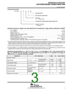
absolute maximum ratings over operating free-air temperature range (unless otherwise noted)
w
V
V
voltage
current
. . . . . . . . . . . . . . . . . . . . . . . . . . . . . . . . . . . . . . . . . . . . . . . . . . . . . . . . . . . . . . . . . . . . . . . . . . . . . 12 V
. . . . . . . . . . . . . . . . . . . . . . . . . . . . . . . . . . . . . . . . . . . . . . . . . . . . . . . . . . . . . . . . . . . . . . . . . . . 30 mA
CC
CC
w
Output current, I
. . . . . . . . . . . . . . . . . . . . . . . . . . . . . . . . . . . . . . . . . . . . . . . . . . . . . . . . . . . . . . . . . . . . . . . . . 1 A
O
Output energy, (Capacitive Load) . . . . . . . . . . . . . . . . . . . . . . . . . . . . . . . . . . . . . . . . . . . . . . . . . . . . . . . . . . . 20 µJ
Analog Inputs (FB, CS) . . . . . . . . . . . . . . . . . . . . . . . . . . . . . . . . . . . . . . . . . . . . . . . . . . . . . . . . . . . . −0.3 V to 6.3 V
Power Dissipation at T < +25_C (D package) . . . . . . . . . . . . . . . . . . . . . . . . . . . . . . . . . . . . . . . . . . . . . . . 0.65 W
A
Storage temperature range, T . . . . . . . . . . . . . . . . . . . . . . . . . . . . . . . . . . . . . . . . . . . . . . . . . . . . −65_C to 150_C
stg
Lead temperature soldering 1,6 mm (1/16 inch) from case for 10 seconds . . . . . . . . . . . . . . . . . . . . . . . 300_C
†
‡
Stresses beyond those listed under “absolute maximum ratings” may cause permanent damage to the device. These are stress ratings only, and
functional operation of the device at these or any other conditions beyond those indicated under “recommended operating conditions” is not
implied. Exposure to absolute-maximum-rated conditions for extended periods may affect device reliability.
Unless otherwise indicated, voltages are reference to ground and currents are positive into and negative out of the specified terminals.
w In normal operation V
is powered through a current limiting resistor. Absolute maximum of 12 V applies when V is driven from a low
CC
CC
impedance source such that I
does not exceed 30 mA (which includes gate drive current requirement).
CC
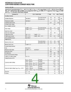
electrical characteristics T = −40_C to 125_C, V
= 10 V (see Note 1), RT = 100 kΩ from REF to
A
CC
RC, CT = 330 pF from RC to GND, 0.1-F capacitor from V
to GND, 0.1-F capacitor from V
to
CC
REF
GND and T = T (unless otherwise stated)
A
J
PARAMETER
Reference Section
TEST CONDITIONS
MIN
TYP
MAX
UNITS
UCC2813-0/1/2/4
UCC2813-3/5
4.925
3.94
5
4
5.075
4.06
30
Output voltage
V
mV
V
I = 0.2 mA to 5 mA
J
Load regulation voltage
Total variation voltage
10
5
UCC2813-0/1/2/4
UCC2813-3/5
4.84
3.84
5.1
See Note 5
4
4.08
f = 10 Hz to 10 kHz,
See Note 7
Output noise voltage
T = 25_C
70
5
µV
J
1000 hours,
See Note 7
Long term stability
T
= 125_C
mV
mA
A
Output short-circuit current
−5
−35
3
POST OFFICE BOX 655303 • DALLAS, TEXAS 75265

 TI [ TEXAS INSTRUMENTS ]