ꢀ ꢁꢁꢂ ꢃ ꢄ ꢅ ꢆꢇꢈ ꢆꢄ ꢈ ꢆꢂꢈ ꢆꢅ ꢈ ꢆꢉ ꢈꢆ ꢊ ꢆꢋ ꢄ
ꢌ ꢍꢎꢆꢏ ꢍꢎꢐꢑ ꢒꢓ ꢁ ꢔꢍꢕ ꢁꢀ ꢑꢑ ꢐꢖꢗꢆꢔꢍ ꢘ ꢐ ꢏꢎ ꢔ
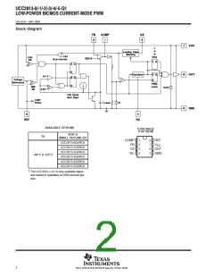
ꢙ
SGLS245 − MAY 2004
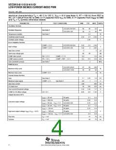
electrical characteristics T = −40_C to 125_C, V
= 10 V (see Note 1), RT = 100 kΩ from REF to
A
CC
RC, CT = 330 pF from RC to GND, 0.1 F capacitor from V
to GND, 0.1 F capacitor from V
to GND
CC
REF
and T = T (unless otherwise stated)
A
J
PARAMETER
TEST CONDITIONS
MIN
TYP
MAX
UNITS
Oscillator Section
UCC2813-0/1/2/4
40
46
52
36
Oscillator frequency
See Note 2
See Note 7
kHz
UCC2813-3/5
26
31
2.5
Temperature stability
%
V
Amplitude peak-to-peak
Oscillator peak voltage
Error Amplifier Section
2.25
2.4
2.55
2.45
V
COMP = 2.5 V
COMP = 2.0 V
UCC2813-0/1/2/4
UCC2813-3/5
2.42
1.92
−2
2.5
2
2.56
2.05
2
Input voltage
V
Input bias current
µA
dB
Open loop voltage gain
COMP sink current
COMP source current
Gain bandwidth product
PWM Section
60
80
FB = 2.7 V,
FB = 1.8 V,
See Note 7
COMP = 1.1 V
COMP = REF − 1.2 V
0.3
3.5
mA
mA
MHz
−0.2
−0.5
2
−0.8
UCC2813-0/2/3
97
48
99
49
100
50
0
Maximum duty cycle
%
%
UCC2813-1/4/5
Minimum duty cycle
Current Sense Section
Gain
COMP = 0 V
See Note 3
1.1
0.9
1.65
1
1.8
1.1
V/V
V
Maximum input signal
Input bias current
COMP = 5 V,
See Note 4
−200
50
200
150
1.7
nA
ns
V
CS blank time
100
1.55
0.9
Over-current threshold voltage
COMP to CS offset voltage
Output Section (OUT)
1.32
0.45
CS = 0 V
1.35
V
I
I
I
I
I
I
I
= 20 mA
All parts
0.1
0.35
0.15
0.7
0.15
1
0.4
0.9
0.4
1.2
0.4
1.9
0.9
70
OUT
OUT
OUT
OUT
OUT
OUT
OUT
= 200 mA
= 50 mA,
= 20 mA,
= −20 mA
= −200 mA
= −50 mA,
All parts
Low-level output voltage
V
V
V
V
= 5 V
= 0 V
UCC2813-3/5
All parts
CC
CC
All parts
All parts
High-level output voltage V
(V - OUT)
SAT CC
V
= 5 V UCC2813-3/5
0.4
41
CC
Rise time
Fall time
C
C
= 1 nF
ns
ns
L
L
= 1 nF
44
75
4
POST OFFICE BOX 655303 • DALLAS, TEXAS 75265

 TI [ TEXAS INSTRUMENTS ]