ꢀ ꢁꢁꢂ ꢃ ꢄ ꢅ ꢆꢇꢈ ꢆꢄ ꢈ ꢆꢂꢈ ꢆꢅ ꢈ ꢆꢉ ꢈꢆ ꢊ ꢆꢋ ꢄ
ꢌ ꢍꢎꢆꢏ ꢍꢎꢐꢑ ꢒꢓ ꢁ ꢔꢍꢕ ꢁꢀ ꢑꢑ ꢐꢖꢗꢆꢔꢍ ꢘ ꢐ ꢏꢎ ꢔ
ꢙ
SGLS245 − MAY 2004
detailed terminal descriptions
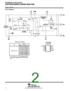
COMP
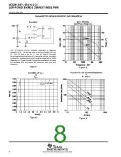
COMP is the output of the error amplifier and the input of the PWM comparator.
Unlike other devices, the error amplifier in the UCC2813 family is a true, low output-impedance, 2-MHz
operational amplifier. As such, the COMP terminal can both source and sink current. However, the error
amplifier is internally current limited, so that one can command zero duty cycle by externally forcing COMP to
GND.
The UCC2813 family features built-in full cycle soft start. Soft start is implemented as a clamp on the maximum
COMP voltage.
CS
CS is the input to the current sense comparators. The UCC2813 family has two different current sense
comparators: the PWM comparator and an overcurrent comparator.
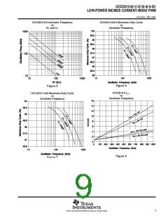
The UCC2813 family contains digital current sense filtering, which disconnects the CS terminal from the current
sense comparator during the 100 ns interval immediately following the rising edge of the OUT pin. This digital
filtering, also called leading-edge blanking, means that in most applications, no analog filtering (RC filter) is
required on CS. Compared to an external RC filter technique, the leading-edge blanking provides a smaller
effective CS to OUT propagation delay. Note, however, that the minimum non-zero on-time of the OUT signal
is directly affected by the leading-edge-blanking and the CS to OUT propagation delay.
The overcurrent comparator is only intended for fault sensing, and exceeding the overcurrent threshold causes
a soft start cycle.
FB
FB is the inverting input of the error amplifier. For best stability, keep FB lead length as short as possible and
FB stray capacitance as small as possible.
ground (GND)
GND is reference ground and power ground for all functions on this part.
OUT
OUT is the output of a high-current power driver capable of driving the gate of a power MOSFET with peak
currents exceeding "750 mA. OUT is actively held low when V
is below the UVLO threshold.
CC
The high-current power driver consists of FET output devices, which can switch all of the way to GND and all
of the way to V . The output stage also provides a low impedance to overshoot and undershoot. This means
CC
that in many cases external Schottky clamp diodes are not required.
6
POST OFFICE BOX 655303 • DALLAS, TEXAS 75265

 TI [ TEXAS INSTRUMENTS ]