UC2906
UC3906
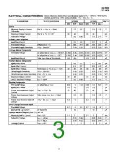
Unless otherwise stated, these specifications apply for TA = -40°C to +70°C for the
UC2906 and 0°C to +70°C for the UC3906, +VIN = 10V, TA = TJ.
ELECTRICAL CHARACTERISTICS:
PARAMETER
TEST CONDITIONS
UC2906
TYP
UC3906
TYP
UNITS
MIN
MAX
MIN
MAX
Driver
Minimum Supply to Source
Differential
Pin 16 = +VIN, IO = 10mA
Pin 16 to Pin 15 = 2V
2.0
2.2
2.0
2.2
V
Maximum Output Current
Saturation Voltage
25
40
25
40
mA
V
0.2
0.45
0.2
0.45
Current Limit Amplifier
Input Bias Current
0.2
250
0.03
1.0
275
0.25
0.2
250
0.03
1.0
275
0.25
µA
mV
%/V
Threshold Voltage
Offset below +VIN
+VIN = 5 to 40V
225
225
Threshold Supply Sensitivity
Voltage Sense Comparator
Threshold Voltage
As a function of VREF, L1 = RESET 0.945 0.95 0.955 0.945 0.95 0.955
V/V
V/V
µA
As a function of VREF, L1 = SET
Total Input Bias at Thresholds
0.895 0.90 0.905 0.895 0.90 0.905
Input Bias Current
Current Sense Comparator
Input Bias Current
-0.5
-0.2
-0.5
-0.2
0.1
0.01
25
0.5
0.2
0.1
0.01
25
0.5
0.2
µA
µA
Input Offset Current
Input Offset Voltage
Referenced to Pin 2, IOUT = 1mA
+VIN = 5 to 40V
20
25
30
20
25
30
mV
%/V
%/V
mA
V
Offset Supply Sensitivity
0.05
0.05
40
0.35
0.35
0.05
0.05
40
0.35
0.35
Offset Common Mode Sensitivity CMV = 2V to +VIN
Maximum Output Current
Output Saturation Voltage
Enable Comparator
Threshold Voltage
VOUT = 2V
IOUT = 10mA
0.2
0.45
1.01
0.2
0.45
1.01
As a function of VREF
0.99
-0.5
25
1.0
-0.2
40
0.99
-0.5
25
1.0
-0.2
40
V/V
µA
Input Bias Current
Trickle Bias Maximum Output
Current
VOUT = +VIN − 3V
mA
Trickle Bias Maximum Output
Voltage
Volts below +VIN, IOUT = 10mA
+VIN = 0V, IOUT = -10µA
2.0
7.0
2.6
1.3
2.0
7.0
2.6
1.3
V
V
Trickle Bias Reverse Hold-Off
Voltage
6.3
0.7
6.3
0.7
Over-Charge Terminate Input
Threshold Voltage
1.0
10
1.0
10
V
Internal Pull-Up Current
At Threshold
µA
Open Collector Outputs (Pins 7, 9, and 10)
Maximum Output Current
Saturation Voltage
VOUT = 2V
2.5
5
2.5
5
mA
V
IOUT = 1.6mA
IOUT = 50µA
VOUT = 40V
0.25
0.03
1
0.45
0.05
3
0.25
0.03
1
0.45
0.05
3
V
Leakage Current
µA
3

 TI [ TEXAS INSTRUMENTS ]