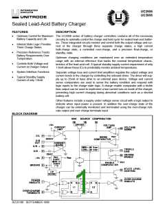
UC2906
UC3906
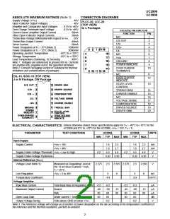
CONNECTION DIAGRAMS
ABSOLUTE MAXIMUM RATINGS (Note 1)
Supply Voltage (+VIN). . . . . . . . . . . . . . . . . . . . . . . . . . . 40V
Open Collector Output Voltages. . . . . . . . . . . . . . . . . . . 40V
Amplifier and Comparator Input Voltages . . . -0.3V to +40V
Over-Charge Terminate Input Voltage. . . . . . -0.3V to +40V
Current Sense Amplifier Output Current . . . . . . . . . . 80mA
Other Open Collector Output Currents. . . . . . . . . . . . 20mA
Trickle Bias Voltage Differential with respect to VIN. . . -32V
Trickle Bias Output Current . . . . . . . . . . . . . . . . . . . . -40mA
Driver Current. . . . . . . . . . . . . . . . . . . . . . . . . . . . . . . 80mA
Power Dissipation at TA = 25°C(Note 2) . . . . . . . . 1000mW
Power Dissipation at TC = 25°C (Note 2). . . . . . . . 2000mW
Operating Junction Temperature . . . . . . . . -55°C to +150°C
Storage Temperature . . . . . . . . . . . . . . . . . -65°C to +150°C
Lead Temperature (Soldering, 10 Seconds) . . . . . . . 300°C
Note 1: Voltages are referenced to ground (Pin 6). Currents
are positive into, negative out of, the specified terminals.
Note 2: Consult Packaging section of Databook for thermal
limitations and considerations of packages.
PLCC-20, LCC-20
(TOP VIEW)
Q, L Packages
PACKAGE PIN FUNCTION
FUNCTION
PIN
1
N/C
C/S OUT
2
C/S-
3
C/S+
4
C/L
N/C
5
6
+VIN
7
GROUND
8
POWER INDICATE
9
OVER CHARGE
TERMINATE
10
N/C
11
12
DIL-16, SOIC-16 (TOP VIEW)
J or N Package, DW Package
OVER CHARGE
INDICATE
STATE LEVEL
CONTROL
13
TRICKLE BIAS
CHARGE ENABLE
N/C
14
15
16
17
18
19
20
VOLTAGE SENSE
COMPENSATION
DRIVER SOURCE
DRIVER SINK
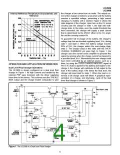
Unless otherwise stated, these specifications apply for TA = -40°C to +70°C for the
UC2906 and 0°C to +70°C for the UC3906, +VIN = 10V, TA = TJ.
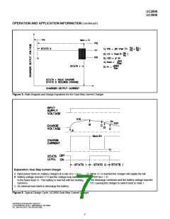
ELECTRICAL CHARACTERISTICS:
PARAMETER
TEST CONDITIONS
UC2906
TYP
UC3906
TYP
UNITS
MIN
MAX
MIN
MAX
Input Supply
Supply Current
+VIN = 10V
+VIN = 40V
1.6
1.8
2.5
2.7
1.6
1.8
2.5
2.7
mA
mA
V
Supply Under-Voltage Threshold +VIN = Low to High
Supply Under-Voltage Hysteresis
4.2
4.5
4.8
4.2
4.5
4.8
0.20
0.30
0.20
0.30
V
Internal Reference (VREF)
Voltage Level (Note 3)
Measured as Regulating Level at
Pin 13 w/ Driver Current = 1mA,
TJ = 25°C
2.275
2.3
2.325 2.270
8
2.3
2.330
8
V
Line Regulation
+VIN = 5 to 40V
3
3
mV
Temperature Coefficient
Voltage Amplifier
-3.9
-3.9
mV/°C
Input Bias Current
Total Input Bias at Regulating Level -0.5
-0.2
-30
60
-0.5
-0.2
-30
60
µA
µA
µA
dB
V
Maximum Output Current
Source
-45
30
50
-15
90
-45
30
50
-15
90
Sink
Open Loop Gain
Driver current = 1mA
Volts above GND or below +VIN
65
65
Output Voltage Swing
0.2
0.2
Note 3. The reference voltage will change as a function of power dissipation on the die according to the temperature coefficient of
the reference and the thermal resistance, junction-to-ambient.
2

 TI [ TEXAS INSTRUMENTS ]