ꢀ ꢁꢂꢃ ꢄꢂ ꢅ
ꢀ ꢁꢂꢃ ꢄꢂ ꢆ
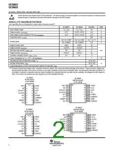
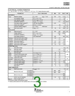
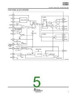
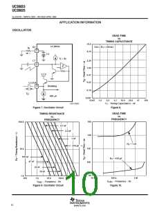
SLUS557B − MARCH 2003 − REVISED APRIL 2004
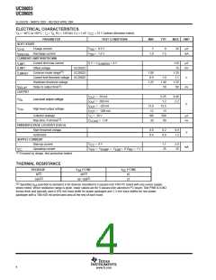
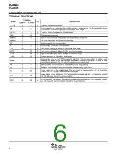
TERMINAL FUNCTIONS
TERMINAL
NAME
I/O
DESCRIPTION
UC28023 UC28025
CLOCK
CT
4
6
4
6
O
I
Output of the internal oscillator
Timing capacitor connection pin for oscillator frequency programming. The timing capacitor should
be connected to the device ground using minimal trace length.
EAOUT
GND
3
10
9
3
10
9
O
−
I
Output of the error amplifier for compensation
Analog ground return pin.
ILIM/SD
ILIMREF
INV
Input to the current limit comparator and the shutdown comparator.
Pin to set the current limit threshold externally.
Inverting input to the error amplifier
11
1
−
I
1
I
NI
2
2
I
Non-inverting input to the error amplifier
OUT
14
−
−
O
O
O
−
High current totem pole output of the on-chip drive stage.
High current totem pole output A of the on-chip drive stage.
High current totem pole output B of the on-chip drive stage.
Ground return pin for the output driver stage
OUTA
OUTB
PGND
11
14
12
−
12
Non-inverting input to the PWM comparator with 1.25-V internal input offset. In voltage mode
operation this serves as the input voltage feed-forward function by using the CT ramp. In peak
current mode operation, this serves as the slope compensation input.
RAMP
7
7
I
RT
SS
5
8
5
8
I
I
Timing resistor connection pin for oscillator frequency programming
Soft-start input pin which also doubles as the maximum duty cycle clamp.
Power supply pin for the output stage. This pin should be bypassed with a 0.1-µF monolithic
VC
13
15
16
13
15
16
−
−
ceramic low ESL capacitor with minimal trace lengths.
Power supply pin for the device. This pin should be bypassed with a 0.1-µF monolithic ceramic
VCC
VREF
low ESL capacitor with minimal trace lengths
5.1−V reference. For stability, the reference should be bypassed with a 0.1-µF monolithic ceramic
O
low ESL capacitor and minimal trace length to the ground plane.
6
www.ti.com

 TI [ TEXAS INSTRUMENTS ]