ꢀ ꢁꢂꢃ ꢄꢂ ꢅ
ꢀ ꢁꢂꢃ ꢄꢂ ꢆ
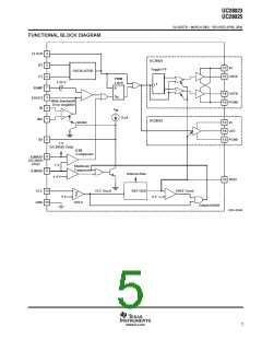
SLUS557B − MARCH 2003 − REVISED APRIL 2004
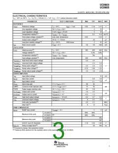
ELECTRICAL CHARACTERISTICS
T
= −40°C to 105°C , T = T
R
= 3.65 kΩ, C = 1 nF, V
CC
= 15 V (unless otherwise noted)
A
J
A,
T
T
PARAMETER
TEST CONDITIONS
MIN
TYP
MAX
UNIT
SOFT-START
I
I
Charge current
Discharge current
V
= 0.5 V
= 1.0 V
3
9
20
µA
CHG
SS
V
SS
1.0
7.5
mA
DISCHG
CURRENT LIMIT/SHUTDOWN
I
Current limit bias current
Offset voltage
0 V < V
(ILIM/SD)
< 4 V
10
15
µA
LIMIT
ILIMIT
UC28023
UC28023
mV
(1)
Common mode range
I
1.00
0.9
1.25
1.1
LIMREF
Current limit threshold voltage UC28025
Shutdown threshold voltage
1.0
1.40
50
V
1.25
1.55
80
(1)
Delay to output time
t
ns
DELAY
OUTPUT
I
I
I
I
= 20 mA
0.25
1.2
13.5
13
0.40
2.2
OUT
OUT
OUT
OUT
V
Low-level output voltage
OL
= 200 mA
= −20 mA
= −200 mA
V
13.0
12
V
OH
High-level output voltage
Collector leakage
V
= 30 V
100
30
500
60
µA
C
(1)
Rise time / Fall time
C
= 1 nF
ns
LOAD
UNDERVOLTAGE LOCKOUT (UVLO)
Start threshold voltage
Hysteresis
8.8
0.4
9.2
0.8
9.6
1.2
V
SUPPLY CURRENT
Start-up current
V
V
= 8 V
1.1
25
2.0
35
CC
mA
I
Operating current
= V
RAMP
= V
ILIM
= 0 V = 1 V
INV
CC
(1)
INV
Ensured by design. Not production tested.
THERMAL RESISTANCE
PACKAGE
θ
JA
(°C/W)
θ
JC
(°C/W)
45
(2)
(2)
90
N
(2)
DW
(2)
50−100
27
(2)
Specified θ (junction-to-ambient) is for devices mountied to 5-square-inch FR4 PC board with one ounce copper
JA
where noted. When resistance range is given, lower values are for 5-square-inch aluminum PC board. Test PWB is 0.062
inches thick and typically uses 0.635 mm trace width for power packages and 1.3 mm trace widths for non-power
packages with a 100x100 mil probe land area at the end of each trace.
4
www.ti.com

 TI [ TEXAS INSTRUMENTS ]