ꢀ ꢁꢂꢃ ꢄꢂ ꢅ
ꢀ ꢁꢂꢃ ꢄꢂ ꢆ
SLUS557B − MARCH 2003 − REVISED APRIL 2004
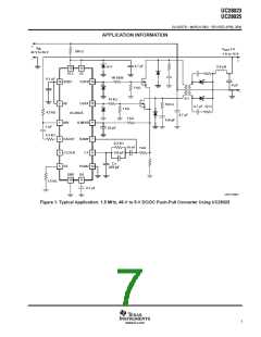
APPLICATION INFORMATION
PCB LAYOUT CONSIDERATIONS
High speed circuits demand careful attention to layout and component placement. To assure proper
performance of the UC2802x follow these rules:
1. Use a ground plane.
2. Damp or clamp parasitic inductive kick energy from the gate of driven MOSFETs. Do not allow the output
pins to ring below ground. A series gate resistor or a shunt 1-A Schottky diode at the output pin serves this
purpose.
3. Bypass VCC, VC, and VREF. Use 0.1-µF monolithic ceramic capacitors with low equivalent series
inductance. Allow less than 1-cm of total lead length for each capacitor between the bypassed pin and the
ground plane.
4. Treat the timing capacitor, C , as a bypass capacitor.
T
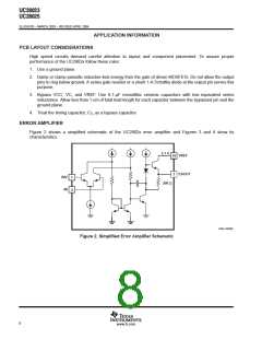
ERROR AMPLIFIER
Figure 2 shows a simplified schematic of the UC2802x error amplifier and Figures 3 and 4 show its
characteristics.
5.1 V
VREF
16
3
EAOUT
INV
NI
1
2
200 Ω
UDG−03049
Figure 2. Simplified Error Amplifier Schematic
8
www.ti.com

 TI [ TEXAS INSTRUMENTS ]