ꢀ ꢁꢂꢃ ꢄꢂ ꢅ
ꢀ ꢁꢂꢃ ꢄꢂ ꢆ
SLUS557B − MARCH 2003 − REVISED APRIL 2004
These devices have limited built-in ESD protection. The leads should be shorted together or the device placed in conductive foam
during storage or handling to prevent electrostatic damage to the MOS gates.
ABSOLUTE MAXIMUM RATINGS
over operating free-air temperature range unless otherwise noted
(1)
UC28023
UC28025
RATING
UNIT
V
Input voltage range,
V
V
V
V
30
C, CC
C, CC
Output current, I
OUT(DC)
OUT
OUT
OUTA, OUTB
OUTA, OUTB
0.5
A
Peak output current, pulsed 0.5 ms I
OUT(pulsed)
2.0
A
Capacitive load, C
200
pF
A
LOAD
INV, NI, RAMP
SS, ILIM/SD
VREF
INV, NI, RAM
SS, ILIM/SD
VREF
−0.3 V to 7 V
Analog inputs
2.0
A
Output current, I
Output current, I
10
REF
CLOCK
SS
CLOCK
SS
−5
CLOCK
Soft-start sink current, I
SINK_SS
5
mA
Output current, I
EAOUT
RT
EAOUT
RT
20
−5
OUT(EA)
Oscillator charging current, I
OSC_CHG
Power Dissipation at T = 25°C (all packages)
1
W
A
Operating junction temperature range, T
−55 to 150
−65 to 150
300
J
Storage temperature, T
stg
°C
Lead temperature 1,6 mm (1/16 inch) from case for 10 seconds, T
sol
(1)
Stresses beyond those listed under “absolute maximum ratings” may cause permanent damage to the device. These are stress ratings only,
and functional operation of the device at these or any other conditions beyond those indicated under “recommended operating conditions” is
not implied. Exposure to absolute-maximum-rated conditions for extended periods may affect device reliability. All voltages are with respect to
GND. All currents are positive into and negative out of the specified terminal.
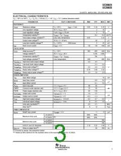
UC28023
N PACKAGE
UC28023
DW PACKAGE
(TOP VIEW)
(TOP VIEW)
1
2
3
4
5
6
7
8
16
15
14
13
12
11
10
9
INV
NI
EAOUT
CLOCK
RT
CT
RAMP
SS
VREF
VCC
OUT
INV
NI
VREF
VCC
OUT
VC
1
2
3
4
5
6
7
8
16
15
14
13
12
EAOUT
CLOCK
RT
VC
PGND
ILIMREF
GND
PGND
CT
11 ILIMREF
10 GND
RAMP
SS
ILIM/SD
9
ILIM/SD
UC28025
UC28025
N PACKAGE
(TOP VIEW)
DW PACKAGE
(TOP VIEW)
1
16
15
14
13
12
11
10
9
INV
VREF
VCC
OUTB
VC
PGND
OUTA
GND
INV
NI
VREF
VCC
2
3
4
5
6
7
8
1
2
3
4
5
6
7
8
16
15
14
13
12
NI
EAOUT
CLOCK
RT
CT
RAMP
SS
EAOUT
CLOCK
RT
OUTB
VC
PGND
CT
11 OUTA
10 GND
ILIM/SD
RAMP
SS
9
ILIM/SD
2
www.ti.com

 TI [ TEXAS INSTRUMENTS ]