TPS929160-Q1
ZHCSNG0 – APRIL 2023
www.ti.com.cn
VLDO1
*
*
RX
OUTA0
OUTA1
RX
RX
OUTA0
OUTA1
VLDO2
4.7µF
VLDO1
4.7µF
VLDO
GND
VLDO
GND
CAN
Transceiver
TX
CANH
CANL
TX
TX
TPS929160-Q1
TPS929160-Q1
VIO
NSTB
EN
NSTB
INH
NSTB
EN
OUTH0
OUTH1
4.7k
OUTH0
OUTH1
100k
ERR
ERR
SUPPLY
SUPPLY
VBAT
FS0
SUPPLY
SUPPLY
VBAT
FS0
VBAT
DC/DC
Converter
4.7µF
4.7µF
ADDR3
ADDR3
10k
FS1
FS2
4.7µF
ADDR2
ADDR1
ADDR0
4.7µF
ADDR2
ADDR1
ADDR0
10k
FS1
FS1
VLDO2
REF
REF
1nF
R(REF)
1nF
R(REF)
: 1nF ceramic capacitor is recommended for each output channel
*
LED Driver
LED
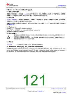
图 8-2. Typical Application Schematic
8.2.2 Design Requirements
Input voltage ranges from 9 V to 16 V, and a total of 80 LED strings with 3 LEDs in each string are required in
one rear-lamp housing. The 80 LED strings must be controlled independently to achieve the animation effect.
The maximum forward voltage of single LED V(F_MAX) = 2.6 V, minimum forward voltage V(F_MIN) = 2.3 V, and
each string current I(LED) = 50 mA. The 48 strings of LED, and 32 strings of LED and MCU must be placed in
three different boards due to the shape of the rear-lamp housing.
8.2.3 Detailed Design Procedure
STEP 1: Determine the architecture at system level.
Because MCU is located in a separate board, the CAN physical layer must be used for off-board long distance
communication between LED driver boards and MCU board. The overall system block diagram is shown in 图
8-1 and the typical schematic for 48 strings of LED board is shown in 图 8-2. The pullup resistors for RX and TX
interface can or cannot required, depending on the model of the CAN transceiver. Normally the pullup resistor
value for RX and TX must be about 10 kΩ. TI recommends putting a 4.7-µF ceramic capacitor on the VLDO
output to keep the voltage stable. Because only one CAN transceiver is required per one PCB board, the CAN
transceiver must only be powered by one LDO output of the TPS929160-Q1. Do not tie the LDO outputs for all
TPS929160-Q1 in one PCB board. TI also recommends placing a 4.7-µF decoupling ceramic capacitor close to
the VBAT and the SUPPLY pin of each TPS929160-Q1 to obtain good EMC performance.
STEP 2: Thermal analysis for the worst application conditions.
Normally the thermal analysis is necessary for linear LED-driver applications to ensure that the operation
junction temperature of TPS929160-Q1 is well managed. The total power consumption on the TPS929160-Q1
itself is one important factor determining operation junction temperature, and it can be calculated by using the
following equation.
P
= V
- V
ìI(CH) ìN(CH)
(MAX)
(SUPPLY _MAX)
(LED _MIN)
(9)
where
•
•
•
•
V(SPPLY_MAX) is maximum supply voltage.
V(LED_MIN) is minimum output voltage.
I(CH) is channel current.
N(CH) is number of used channels.
Based on the worst-case analysis for maximum power consumption on device, either optimizing PCB layout for
better power dissipation as Layout Example describes or implementing a DC-to-DC converter in previous stage
on MCU board can be considered. The DC-to-DC such as a buck converter or buck-boost converter can regulate
the battery voltage to be a stable supply for the TPS929160-Q1 with sufficient headroom. A properly designed
supply voltage is helpful to minimize the power consumption on the TPS929160-Q1 itself as well as the whole
Copyright © 2023 Texas Instruments Incorporated
Submit Document Feedback
117
Product Folder Links: TPS929160-Q1
English Data Sheet: SLVSG60

 TI [ TEXAS INSTRUMENTS ]