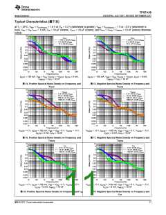
TPS7A39
www.ti.com.cn
ZHCSGP0A –JULY 2017–REVISED SEPTEMBER 2017
Electrical Characteristics (continued)
at TJ = –40°C to +125°C, VINP(nom) = VOUTP(nom) + 1 V or VIN(nom) = 3.3 V (whichever is greater), VINN(nom) = VOUTN(nom) – 1 V or
VINN(nom) = –3.3 V (whichever is less), VEN = VINP, IOUT = 1 mA, CINx = 2.2 μF, COUTx = 10 μF, CFFx = CNR/SS = open, R1N = R2N
10 kΩ, and FBP tied to OUTP (unless otherwise noted); typical values are at TJ = 25°C
=
PARAMETER
TEST CONDITIONS
MIN
TYP
MAX
UNIT
Positive channel
Negative channel
5.5
100
Feedback pin leakage
current
IFBx
nA
–100
3
–9.7
5.1
INR/SS
IEN
VIH(EN)
VIL(EN)
Soft-start charging current
Enable pin leakage current
Enable high-level voltage
Enable low-level voltage
VNR/SS = 0.9 V
6.7
1
µA
µA
V
VEN = VINP = 33 V
0.02
2.2
0
VINP
0.4
V
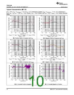
|VIN| = 6 V, |VOUT(nom)| = 5 V, COUT = 10 μF,
CNR/SS = CFF= 10 nF, f = 120 Hz
PSRR
Power-supply rejection ratio
69
20.63
26.86
22.13
28.68
dB
VINP = 3.3 V, VOUTP(nom) = VNR/SS, COUTP = 10 μF,
CNR/SS = 10 nF, BW = 10 Hz to 100 kHz
Positive channel
Negative channel
VINP = 6 V, VOUTP(nom) = 5 V, COUTP = 10 μF,
CNR/SS = CFF = 10 nF, BW = 10 Hz to 100 kHz
Vn
Output noise voltage
µVRMS
VINN = –3 V, VOUTN(nom) = –VNR/SS, COUTP = 10 μF,
CNR/SS = 10 nF, BW = 10 Hz to 100 kHz
VINN = –6 V, VOUTN(nom) = –5 V, COUTP = 10 μF,
CNR/SS = CFF= 10 nF, BW = 10 Hz to 100 kHz
RNR/SS
Tsd
Filter resistor from band gap to NR pin
Thermal shutdown temperature
350
175
160
kΩ
Shutdown, temperature increasing
Reset, temperature decreasing
°C
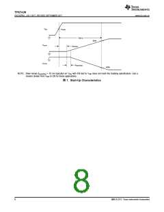
6.6 Startup Characteristics
at TJ = –40°C to +125°C, VINP(nom) = VOUTP(nom) + 1 V or VIN(nom) = 3.3 V (whichever is greater), VINN(nom) = VOUTN(nom) – 1 V or
VINN(nom) = –3.3 V (whichever is less), VEN = VINP, IOUT = 1 mA, CINx = 2.2 μF, COUTx = 10 μF, CFFx = CNR/SS = 4.7nF, R1N = R2N
= 10 kΩ, and FBP tied to OUTP (unless otherwise noted); typical values are at TJ = 25°C
PARAMETER
TEST CONDITIONS
MIN
TYP
MAX UNIT
Delay time from EN low-to-high transition to 2.5%
VOUTP
From EN low-to-high transition to VOUTP = 2.5% ×
VOUTP(nom)
tEN(delay)
tstart-up
300
µs
Delay time from EN low-to-high transition to both
outputs reaching 95% of final value
From EN low-to-high transition to VOUTP
=
1.1
ms
VOUTP(nom) × 95% and VOUTN = VOUTN(nom) × 95%
Delay time from VOUTP leaving a high-impedance
state to VOUTN leaving a high-impedance state
From VOUTP = VOUTP(nom) × 2.5% to VOUTN
VOUTN(nom) × 2.5%
=
tPstart-Nstart
–40
–17
75
40
µs
Δ|VOUTP
VOUTN
–
Voltage difference between the positive and
negative output
During tPstart-Nstart
300
mV
|
版权 © 2017, Texas Instruments Incorporated
7

 TI [ TEXAS INSTRUMENTS ]