TPS7A39
ZHCSGP0A –JULY 2017–REVISED SEPTEMBER 2017
www.ti.com.cn
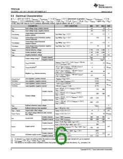
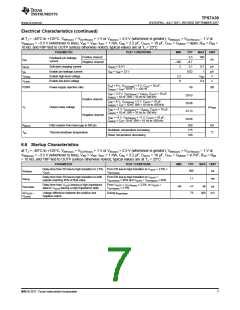
6.5 Electrical Characteristics
at TJ = –40°C to +125°C, VINP(nom) = VOUTP(nom) + 1 V or VIN(nom) = 3.3 V (whichever is greater), VINN(nom) = VOUTN(nom) – 1 V or
VINN(nom) = –3.3 V (whichever is less), VEN = VINP, IOUT = 1 mA, CINx = 2.2 μF, COUTx = 10 μF, CFFx = CNR/SS = open, R1N = R2N
10 kΩ, and FBP tied to OUTP (unless otherwise noted); typical values are at TJ = 25°C
=
PARAMETER
TEST CONDITIONS
MIN
TYP
MAX
UNIT
VINP
VINN
Input voltage range, positive channel
Input voltage range, negative channel
3.3
33
V
–33
–3.3
V
Undervoltage lockout threshold,
positive channel
VUVLOP(rising)
VUVLOP(hys)
VINP rising, VINN = –3.3 V
1.4
3.1
V
Undervoltage lockout threshold, positive
channel hysteresis
VINP falling, VINN = –3.3 V
120
70
mV
Undervoltage lockout threshold,
negative channel
VUVLON(falling)
VUVLON(hys)
VINN falling, VINP = 3.3 V
VINN rising, VINP = 3.3 V
–3.1
–1.4
V
Undervoltage lockout threshold, negative
channel, hysteresis
mV
VNR/SS
VFBP
Internal reference voltage
Positive feedback voltage
Negative feedback voltage
1.172
1.170
–10
1.19
1.188
3.7
1.208
1.206
10
V
V
VFBN
mV
Positive channel
Output voltage range(1)
VFBP
–30
30
V
(2)
Negative channel
VFBN
V
INP(nom) ≤ VINP ≤ 33 V, 1 mA ≤ IOUTP ≤ 150 mA,
VOUTP accuracy
–1.5
–3
1.5 %VOUT
1.2 V ≤ VOUTP(nom) ≤ 30 V
–33 V ≤ VINN ≤ VINN(nom), –150 mA ≤ IOUTN
–1 mA, –30 V ≤ VOUTN(nom) ≤ –1.2 V
≤
VOUTN accuracy(3)
3
36
12
%VOUT
mV
VOUT
–33 V ≤ VINN ≤ VINN(nom) , –150 mA ≤ IOUTN
1 mA, –1.2 V < VOUTN(nom) < 0 V
≤
–36
–12
Negative VOUT channel accuracy
–33 V ≤ VINN ≤ VINN(nom) , –150 mA ≤ IOUTN
1 mA, VOUTN(nom) = 0 V
≤
Line regulation, positive channel
Line regulation, negative channel
Load regulation, positive channel
Load regulation, negative channel
V
INP(nom) ≤ VINP ≤ 33 V
0.035
0.125
–0.09
0.715
ΔVOUT(ΔVIN) /
VOUT(NOM)
%VOUT
%VOUT
–33 V ≤ VINN ≤ VOUT(nom) + 1 V
1 mA ≤ IOUTP ≤ 150 mA
ΔVOUT(ΔIOUT) /
VOUT(NOM)
–150 mA ≤ IOUTN ≤ –1 mA
IOUTP = 50 mA, 3.3 V ≤ VINP(nom) ≤ 33.0 V,
VFBP = 1.070 V
175
300
300
500
Positive channel
IOUTP = 150 mA, 3.3 V ≤ VINP(nom) ≤ 33.0 V,
VFBP = 1.070 V
VDO
Dropout voltage
mV
IOUTN = –50 mA, –3.3 V ≤ VINN(nom) ≤ –33.0 V,
VFBN = 0.0695 V
–250
–400
–145
–275
Negative channel
IOUTN = –150 mA, –3.3 V ≤ VINN(nom) ≤ –33.0 V,
VFBN = 0.0695 V
VBUF
Buffered reference output voltage
Buffered reference load regulation
Output buffer offset voltage
VNR/SS
V
VBUF/IBUF
VBUF – VNR/SS
IBUF = 100 µA to 1 mA
VNR/SS = 0.25 V to 1.2 V
1
3
mV/mA
mV
–4
8
DC output voltage difference with a forced
REF voltage
VOUTP–VOUTN
VNR/SS = 0.25 V to 1.2 V
VOUTP = 90% VOUTP(nom)
–10
10 %VNR/SS
500
Positive channel
Current limit
200
330
–300
75
ILIM
mA
µA
µA
Negative channel VOUTN = 90% VOUTN(nom)
–500
–200
150
IOUTP = 0 mA, R2N = open, VINP = 33 V
IOUTP = 150 mA, R2N = open, VINP = 33 V
Positive channel
904
ISUPPLY
Supply current
IOUTN = 0 mA, VOUTN(nom)= 0 V, R2N = open, VINN
–33 V
=
–150
–4.5
–60
Negative channel
IOUTN = 150 mA, R2N = open, VINN = –33 V
VEN = 0.4 V, VINP = 33 V
–1053
3.75
Positive channel
6.5
ISHDN
Shutdown supply current
Negative channel VEN = 0.4 V, VINN = –33 V
–2.25
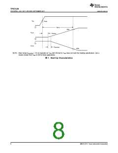
(1) To ensure VOUT does not drift up while the device is disabled, a minimum load current of 5 µA is required.
(2) VOUT(target) = 0 V, R1N = 10 kΩ, R2N = open.
(3) The device is not tested under conditions where the power dissipated across the device, PD, exceeds 2 W.
6
Copyright © 2017, Texas Instruments Incorporated

 TI [ TEXAS INSTRUMENTS ]