TPS7A39
www.ti.com.cn
ZHCSGP0A –JULY 2017–REVISED SEPTEMBER 2017
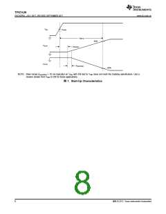
5 Pin Configuration and Functions
DSC Package
10-Pin WSON
Top View
INP
EN
1
2
3
4
5
10
9
OUTP
FBP
Thermal Pad
NR/SS
GND
INN
8
BUF
FBN
OUTN
7
6
Not to scale
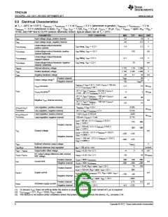
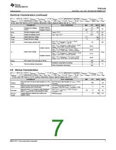
Pin Functions
PIN
NAME
I/O
DESCRIPTION
NO.
Positive input. A 10-μF(1) or larger capacitor must be tied from this pin to ground to ensure stability.
Place the input capacitor as close to the input as possible; see the Capacitor Recommendations section
for more information.
1
2
INP
I
Enable pin. Driving this pin to logic high (VEN ≥ VIH(EN)) enables the device; driving this pin to logic low
(VEN ≤ VIL(EN)) disables the device. If enable functionality is not required, this pin must be connected to
INP; see the Application and Implementation section for more detail. The enable voltage cannot exceed
the input voltage (VEN ≤ VINP).
EN
I
Noise-reduction, soft-start pin. Connecting an external capacitor between this pin and ground reduces
reference voltage noise and enables soft-start and start-up tracking. A 10-nF or larger capacitor (CNR/SS
is recommended to be connected from NR/SS to GND to maximize or optimize ac performance and to
ensure start-up tracking. This pin can also be driven externally to provide greater output voltage
accuracy and lower noise, see the User-Settable Buffered Reference section for more information.
)
3
NR/SS
—
Ground pin. This pin must be connected to ground and the thermal pad with a low-impedance
connection.
Negative input. A 10-μF(1) or larger capacitor must be tied from this pin to ground to ensure stability.
Place the input capacitor as close to the input as possible; see the Capacitor Recommendations section
for more information.
4
5
GND
INN
—
I
Negative output. A 10-μF(1) or larger capacitor must be tied from this pin to ground to ensure stability.
Place the output capacitor as close to the output as possible; see the Capacitor Recommendations
section for more information.
6
7
8
OUTN
FBN
O
I
Negative output feedback pin. This pin is used to set the negative output voltage. Although not required,
a 10-nF feed-forward capacitor from FBN to OUTN (as close to the device as possible) is recommended
to maximize ac performance. Nominally this pin is regulated to VFBN. Do not connect to ground.
Buffered reference output. This pin is connected to FBN through R2 and the voltage at this node is
inverted and scaled up by the negative feedback network to provide the desired output voltage. The
buffered reference can be used to drive external circuits, and has a 1-mA maximum load.
BUF
O
Positive output feedback pin. This pin is used to set the positive output voltage. Although not required, a
10-nF feed-forward capacitor from FBP to OUTP (as close to the device as possible) is recommended to
maximize ac performance. Nominally this pin is regulated to VFBP. Do not connect this pin directly to
ground.
9
FBP
I
Positive output. A 10-μF(1) or larger capacitor must be tied from this pin to ground to ensure stability.
Place the output capacitor as close to the output as possible; see the Capacitor Recommendations
section for more information.
10
OUTP
O
Pad
Thermal Pad
—
Connect the thermal pad to a large-area ground plane. The thermal pad is internally connected to GND.
(1) The nominal input and output capacitance must be greater than 2.2 µF; throughout this document the nominal derating on these
capacitors is 80%. Take care to ensure that the effective capacitance at the pin is greater than 2.2 µF.
Copyright © 2017, Texas Instruments Incorporated
3

 TI [ TEXAS INSTRUMENTS ]