TPS7A39
ZHCSGP0A –JULY 2017–REVISED SEPTEMBER 2017
www.ti.com.cn
6 Specifications
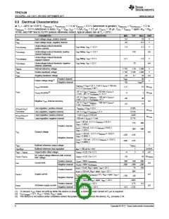
6.1 Absolute Maximum Ratings
over operating junction temperature range (unless otherwise noted)(1)(2)
MIN
–0.3
MAX
36
UNIT
INP
INN
–36
0.3
OUTP
OUTN
–0.3
VINN – 0.3(4)
VINP + 0.3(3)
0.3
Voltage
FBP
BUF
NR/SS
FBN
EN
–0.3
VINP + 0.3(5)
VINP + 0.3(5)
VINP + 0.3(6)
0.3
V
–1
–0.3
VINN – 0.3(7)
–0.3
VINP + 0.3(8)
Internally
limited
Output current
Current
Buffer current
2
mA
°C
Operating junction temperature, TJ
Storage, Tstg
–55
–65
150
150
Temperature
(1) Stresses beyond those listed under Absolute Maximum Ratings may cause permanent damage to the device. These are stress ratings
only, which do not imply functional operation of the device at these or any other conditions beyond those indicated under Recommended
Operating Conditions. Exposure to absolute-maximum-rated conditions for extended periods may affect device reliability.
(2) All voltages with respect to the ground pin, unless otherwise noted.
(3) The absolute maximum rating is VINP + 0.3 V or 33 V, whichever is smaller.
(4) The absolute maximum rating is VINN – 0.3 V or –33 V, whichever is greater.
(5) The absolute maximum rating is VINP + 0.3 V or 3 V, whichever is smaller.
(6) The absolute maximum rating is VINP + 0.3 V or 2 V, whichever is smaller.
(7) The absolute maximum rating is VINN – 0.3 V or –3 V, whichever is greater.
(8) The absolute maximum rating is VINP + 0.3 V or 36 V, whichever is smaller.
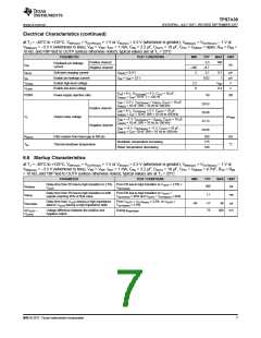
6.2 ESD Ratings
VALUE
±1000
±500
UNIT
Human-body model (HBM), per ANSI/ESDA/JEDEC JS-001(1)
Charged-device model (CDM), per JEDEC specification JESD22-C101(2)
VESD
Electrostatic discharge
V
(1) JEDEC document JEP155 states that 500-V HBM allows safe manufacturing with a standard ESD control process.
(2) JEDEC document JEP157 states that 250-V CDM allows safe manufacturing with a standard ESD control process.
4
Copyright © 2017, Texas Instruments Incorporated

 TI [ TEXAS INSTRUMENTS ]