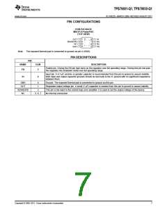
TPS79801-Q1, TPS79850-Q1
www.ti.com
SLVS822D –MARCH 2009–REVISED AUGUST 2011
APPLICATION INFORMATION
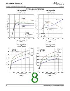
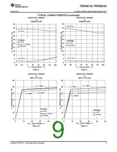
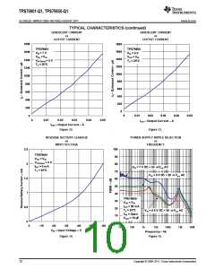
The TPS798xx is a 50-mA high-voltage LDO regulator with micropower quiescent current and shutdown. The
device is capable of supplying 50 mA at a dropout voltage of 300 mV (typ). The low operating quiescent current
(40 μA) drops to 1 μA in shutdown. In addition to the low quiescent current, the TPS798xx incorporates several
protection features that make it ideal for battery-powered applications.
The device is protected against both reverse-input and reverse-output voltages. In battery-backup applications,
where the output can be held up by a backup battery when the input is pulled to ground, the TPS798xx acts as if
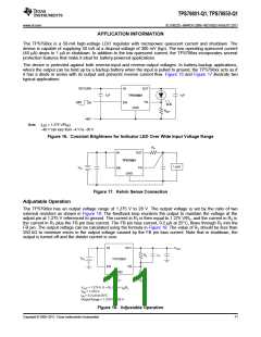
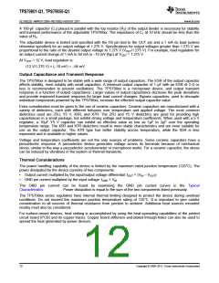
it has a diode in series with its output and prevents reverse current flow. Figure 16 and Figure 17 illustrate two
typical applications.
RETURN
IN
OUT
TPS79801
1mF
1mF
FB
EN
OFF
ON
GND
RSET
-48V
Note: ILED = 1.275 V/RSET
–48 V can vary from –4 V to –50 V
Figure 16. Constant Brightness for Indicator LED Over Wide Input Voltage Range
RP
IN
OUT
TPS79801
Load
VIN
FB
EN
GND
Figure 17. Kelvin Sense Connection
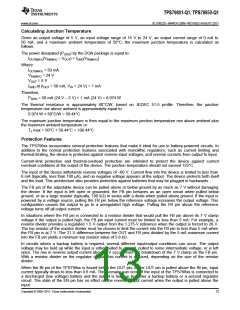
Adjustable Operation
The TPS798xx has an output voltage range of 1.275 V to 28 V. The output voltage is set by the ratio of two
external resistors as shown in Figure 18. The feedback loop monitors the output to maintain the voltage at the
adjust pin at 1.275 V referenced to ground. The current in R1 is then equal to 1.275 V/R1, and the current in R2 is
the current in R1 plus the FB pin bias current. The FB pin bias current, 0.2 μA at 25°C, flows through R2 into the
FB pin. The output voltage can be calculated using the formula in Figure 18. The value of R1 should be less than
250 kΩ to minimize errors in the output voltage caused by the FB pin bias current. Note that in shutdown, the
output is turned off and the divider current is zero.
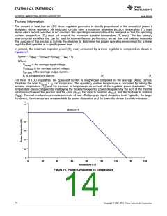
VOUT
IN
OUT
R2
C1
VIN
TPS79801
EN
FB
GND
R1
VOUT = 1.275 V (1 + R2 / R1) + IFBR2
VFB = 1.275 V
IFB = 0.2 µA at 25°C
Output Range = 1.275 V to 28 V
Figure 18. Adjustable Operation
Copyright © 2009–2011, Texas Instruments Incorporated
11

 TI [ TEXAS INSTRUMENTS ]