TPS79801-Q1, TPS79850-Q1
SLVS822D –MARCH 2009–REVISED AUGUST 2011
www.ti.com
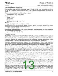
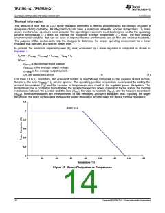
Thermal Information
The amount of heat that an LDO linear regulator generates is directly proportional to the amount of power it
dissipates during operation. All integrated circuits have a maximum allowable junction temperature (TJ max)
above which normal operation is not assured. The operating environment must be designed so that the operating
junction temperature (TJ) does not exceed the maximum junction temperature (TJ max). The two primary
environmental variables that can be used to improve thermal performance are air flow and external heatsinks.
The purpose of this section is to help the designer to determine the proper operating environment for a linear
regulator that operates at a specific power level.
In general, the maximum expected power (PD max) consumed by a linear regulator is computed as shown in
Equation 1:
PDmax = (VIN(avg) – VOUT(avg)) × IOUT(avg) + VI(avg) × IQ
Where:
VIN(avg) is the average input voltage.
VOUT(avg) is the average output voltage.
IOUT(avg) is the average output current.
IQ is the quiescent current.
(1)
(1)
For most TI LDO regulators, the quiescent current is insignificant compared to the average output current;
therefore, the term VIN(avg) × IQ can be ignored. The operating junction temperature is computed by adding the
ambient temperature (TA) and the increase in temperature as a result of the regulator power dissipation. The
temperature rise is computed by multiplying the maximum expected power dissipation by the sum of the thermal
resistances between the junction and the case (RθJC), the case to heatsink (RθCS), and the heatsink to ambient
(RθSA). Thermal resistances are measurements of how effectively an object dissipates heat. Typically, the larger
the device, the more surface area available for power dissipation and the lower the device thermal resistance.
1.2
JEDEC 51-5
1
0.8
0.6
0.4
0.2
0
0
20
40
60
80
100
120
140
160
Temperature (°C)
Figure 19. Power Dissipation vs Temperature
14
Copyright © 2009–2011, Texas Instruments Incorporated

 TI [ TEXAS INSTRUMENTS ]