TPS79801-Q1, TPS79850-Q1
www.ti.com
SLVS822D –MARCH 2009–REVISED AUGUST 2011
Calculating Junction Temperature
Given an output voltage of 5 V, an input voltage range of 15 V to 24 V, an output current range of 0 mA to
50 mA, and a maximum ambient temperature of 50°C, the maximum junction temperature is calculated as
follows.
The power dissipated (PDISS) by the DGN package is equal to:
IOUT(MAX)(VIN(MAX) – VOUT) + IGND(VIN(MAX)
)
Where:
IOUT(MAX) = 50 mA
VIN(MAX) = 24 V
VOUT = 5 V
IGND at (IOUT = 50 mA, VIN = 24 V) = 1 mA
Therefore,
PDISS = 50 mA (24 V – 5 V) + 1 mA (24 V) = 0.974 W
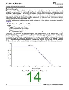
The thermal resistance is approximately 60°C/W, based on JEDEC 51-5 profile. Therefore, the junction
temperature rise above ambient is approximately equal to:
0.974 W × 60°C/W = 58.44°C
The maximum junction temperature is then equal to the maximum junction temperature rise above ambient plus
the maximum ambient temperature or:
TJ max = 50°C + 58.44°C = 108.44°C
Protection Features
The TPS798xx incorporates several protection features that make it ideal for use in battery-powered circuits. In
addition to the normal protection features associated with monolithic regulators, such as current limiting and
thermal limiting, the device is protected against reverse-input voltages, and reverse currents from output to input.
Current-limit protection and thermal-overload protection are intended to protect the device against current
overload conditions at the output of the device. The junction temperature should not exceed 125°C.
The input of the device withstands reverse voltages of –60 V. Current flow into the device is limited to less than
6 mA (typically, less than 100 μA), and no negative voltage appears at the output. The device protects both itself
and the load. This architecture also provides protection against batteries that may be plugged in backwards.
The FB pin of the adjustable device can be pulled above or below ground by as much as 7 V without damaging
the device. If the input is left open or grounded, the FB pin behaves as an open circuit when pulled below
ground, or as a large resistor (typically, 100 kΩ) in series with a diode when pulled above ground. If the input is
powered by a voltage source, pulling the FB pin below the reference voltage increases the output voltage. This
configuration causes the output to go to a unregulated high voltage. Pulling the FB pin above the reference
voltage turns off all output current.
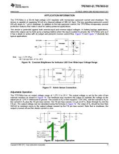
In situations where the FB pin is connected to a resistor divider that would pull the FB pin above its 7 V clamp
voltage if the output is pulled high, the FB pin input current must be limited to less than 5 mA. For example, a
resistor divider provides a regulated 1.5 V output from the 1.275-V reference when the output is forced to 28 V.
The top resistor of the resistor divider must be chosen to limit the current into the FB pin to less than 5 mA when
the FB pin is at 7 V. The 21-V difference between the OUT and FB pins divided by the 5-mA maximum current
into the FB pin yields a minimum top resistor value of 5.8 kΩ.
In circuits where a backup battery is required, several different input/output conditions can occur. The output
voltage may be held up while the input is either pulled to ground, pulled to some intermediate voltage, or is left
open. The rise in reverse output current above 7 V occurs from the breakdown of the 7 V clamp on the FB pin.
With a resistor divider on the regulator output, this current is reduced, depending on the size of the resistor
divider.
When the IN pin of the TPS798xx is forced below the OUT pin, or the OUT pin is pulled above the IN pin, input
current typically drops to less than 0.6 mA. This scenario can occur if the input of the TPS798xx is connected to
a discharged (low voltage) battery and the output is held up by either a backup battery or a second regulator
circuit. The state of the EN pin has no effect on the reverse output current when the output is pulled above the
input.
Copyright © 2009–2011, Texas Instruments Incorporated
13

 TI [ TEXAS INSTRUMENTS ]