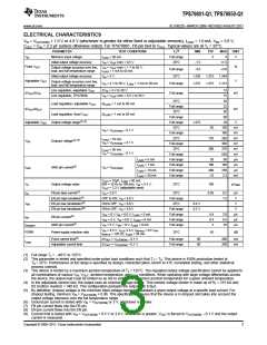
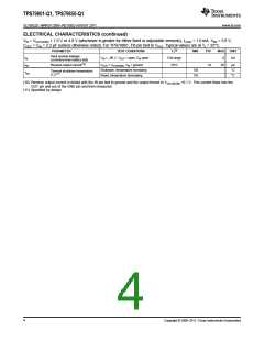
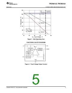
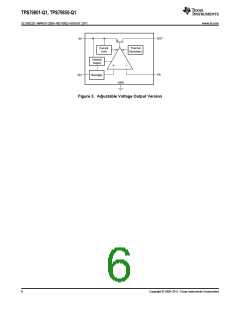
TPS79801-Q1, TPS79850-Q1
www.ti.com
SLVS822D –MARCH 2009–REVISED AUGUST 2011
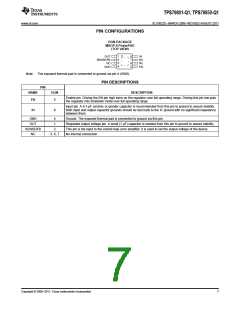
PIN CONFIGURATIONS
DGN PACKAGE
MSOP-8 PowerPAD
(TOP VIEW)
1
2
3
4
OUT
SENSE/FB
NC
8
7
6
5
IN
NC
NC
EN
GND
Note: The exposed thermal pad is connected to ground via pin 4 (GND).
PIN DESCRIPTIONS
PIN
NAME
DGN
DESCRIPTION
Enable pin. Driving the EN pin high turns on the regulator over full operating range. Driving this pin low puts
the regulator into shutdown mode over full operating range.
EN
5
Input pin. A 0.1-μF ceramic or greater capacitor is recommended from this pin to ground to assure stability.
Both input and output capacitor grounds should be tied back to the IC ground with no significant impedance
between them.
IN
8
GND
OUT
4
Ground. The exposed thermal pad is connected to ground via this pin.
Regulated output voltage pin. A small (1 μF) capacitor is needed from this pin to ground to assure stability.
This pin is the input to the control loop error amplifier; it is used to set the output voltage of the device.
No internal connection
1
2
SENSE/FB
NC
3, 6, 7
Copyright © 2009–2011, Texas Instruments Incorporated
7

 TI [ TEXAS INSTRUMENTS ]