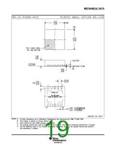
TPS74801-Q1
www.ti.com
SLVSAI4A –OCTOBER 2010–REVISED FEBRUARY 2011
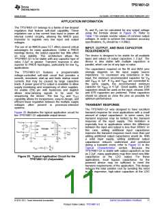
Figure 29 shows the variation of θJA as a function of
ground plane copper area in the board. It is intended
only as a guideline to demonstrate the effects of heat
spreading in the ground plane and should not be
used to estimate actual thermal performance in real
application environments.
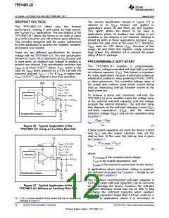
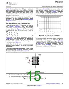
By looking at Figure 30, the new thermal metrics (ΨJT
and ΨJB) have very little dependency on board size.
That is, using ΨJT or ΨJB with Equation 6 is a good
way to estimate TJ by simply measuring TT or TB,
regardless of the application board size.
12
NOTE: When the device is mounted on an
application PCB, it is strongly recommended to use
ΨJT and ΨJB, as explained in the Estimating Junction
Temperature section.
YJB
10
8
6
4
ESTIMATING JUNCTION TEMPERATURE
Using the thermal metrics ΨJT and ΨJB, as shown in
the Thermal Information table, the junction
temperature can be estimated with corresponding
formulas (given in Equation 6). For backwards
compatibility, an older θJC,Top parameter is listed as
well.
2
YJT
0
0
1
2
3
4
5
6
7
8
9
10
Board Copper Area (in2)
YJT: TJ = TT + YJT · PD
YJB: TJ = TB + YJB · PD
(6)
Figure 30. ΨJT and ΨJB vs Board Size
Where PD is the power dissipation shown by
Equation 4, TT is the temperature at the center-top of
the IC package, and TB is the PCB temperature
measured 1mm away from the IC package on the
PCB surface (see Figure 31).
For a more detailed discussion of why TI does not
recommend using θJC(top) to determine thermal
characteristics, refer to application report SBVA025,
Using New Thermal Metrics, available for download
at www.ti.com. For further information, refer to
application report SPRA953, IC Package Thermal
Metrics, also available on the TI website.
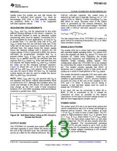
NOTE: Both TT and TB can be measured on actual
application boards using a thermo-gun (an infrared
thermometer).
For more information about measuring TT and TB, see
the application note SBVA025, Using New Thermal
Metrics, available for download at www.ti.com.
TT on top
of IC(1)
TB on PCB
surface(2)
1mm
Example DRC (SON) Package Measurement
(1) TT is measured at the center of both the X- and Y-dimensional axes.
(2) TB is measured below the package lead on the PCB surface.
Figure 31. Measuring Points for TT and TB
© 2010–2011, Texas Instruments Incorporated
Submit Documentation Feedback
15
Product Folder Link(s): TPS74801-Q1

 TI [ TEXAS INSTRUMENTS ]