TPS74801-Q1
www.ti.com
SLVSAI4A –OCTOBER 2010–REVISED FEBRUARY 2011
APPLICATION INFORMATION
The TPS74801-Q1 belongs to a family of low dropout
regulators that feature soft-start capability. These
regulators use a low current bias input to power all
internal control circuitry, allowing the NMOS pass
transistor to regulate very low input and output
voltages.
R1 and R2 can be calculated for any output voltage
using the formula shown in Figure 25. Refer to
Table 1 for sample resistor values of common output
voltages. In order to achieve the maximum accuracy
specifications, R2 should be ≤ 4.99kΩ.
The use of an NMOS-pass FET offers several critical
advantages for many applications. Unlike a PMOS
topology device, the output capacitor has little effect
on loop stability. This architecture allows the
TPS74801-Q1 to be stable with any capacitor type of
value 2.2μF or greater. Transient response is also
superior to PMOS topologies, particularly for low VIN
applications.
INPUT, OUTPUT, AND BIAS CAPACITOR
REQUIREMENTS
The device is designed to be stable for all available
types and values of output capacitors ≥ 2.2μF. The
device is also stable with multiple capacitors in
parallel, which can be of any type or value.
The capacitance required on the IN and BIAS pins
strongly depends on the input supply source
impedance. To counteract any inductance in the
input, the minimum recommended capacitor for VIN
and VBIAS is 1μF. If VIN and VBIAS are connected to
the same supply, the recommended minimum
capacitor for VBIAS is 4.7μF. Good quality, low ESR
capacitors should be used on the input; ceramic X5R
and X7R capacitors are preferred. These capacitors
should be placed as close the pins as possible for
optimum performance.
The TPS74801-Q1 features
a
programmable
voltage-controlled soft-start circuit that provides a
smooth, monotonic start-up and limits startup inrush
currents that may be caused by large capacitive
loads. A power good (PG) output is available to allow
supply monitoring and sequencing of other supplies.
An enable (EN) pin with hysteresis and deglitch
allows slow-ramping signals to be used for
sequencing the device. The low VIN and VOUT
capability allows for inexpensive, easy-to-design, and
efficient linear regulation between the multiple supply
voltages often present in processor-intensive
systems.
TRANSIENT RESPONSE
The TPS74801-Q1 was designed to have excellent
transient response for most applications with a small
amount of output capacitance. In some cases, the
transient response may be limited by the transient
response of the input supply. This limitation is
especially true in applications where the difference
between the input and output is less than 300mV. In
this case, adding additional input capacitance
improves the transient response much more than just
adding additional output capacitance would do. With
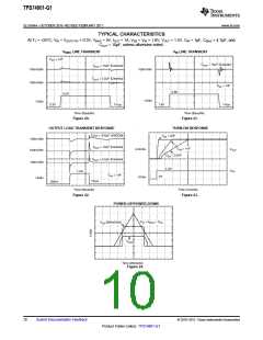
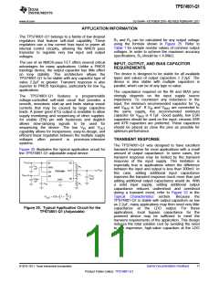
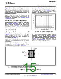
Figure 25 illustrates the typical application circuit for
the TPS74801-Q1 adjustable output device.
VIN
IN
PG
CIN
R3
R1
BIAS
EN
SS
1mF
VOUT
OUT
TPS74801
VBIAS
COUT
CBIAS
10mF
FB
GND
1mF
CSS
R2
a
solid input supply, adding additional output
capacitance reduces undershoot and overshoot
during a transient event; refer to Figure 22 in the
Typical Characteristics section. Because the
TPS74801-Q1 is stable with output capacitors as low
as 2.2μF, many applications may then need very little
capacitance at the LDO output. For these
applications, local bypass capacitance for the
powered device may be sufficient to meet the
transient requirements of the application. This design
reduces the total solution cost by avoiding the need
to use expensive, high-value capacitors at the LDO
output.
R1
VOUT = 0.8 ´ 1 +
(
)
R2
Figure 25. Typical Application Circuit for the
TPS74801-Q1 (Adjustable)
© 2010–2011, Texas Instruments Incorporated
Submit Documentation Feedback
11
Product Folder Link(s): TPS74801-Q1

 TI [ TEXAS INSTRUMENTS ]