TPS74801-Q1
SLVSAI4A –OCTOBER 2010–REVISED FEBRUARY 2011
www.ti.com
INTERNAL CURRENT LIMIT
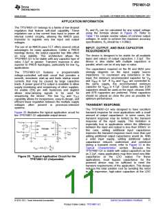
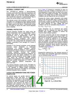
R1 in Figure 25 should be connected as close as
possible to the load. If BIAS is connected to IN, it is
recommended to connect BIAS as close to the sense
point of the input supply as possible. This connection
minimizes the voltage drop on BIAS during transient
conditions and can improve the turn-on response.
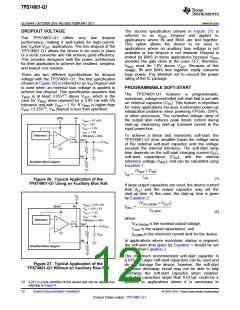
The TPS74801-Q1 features
a
factory-trimmed,
accurate current limit that is flat over temperature and
supply voltage. The current limit allows the device to
supply surges of up to 2A and maintain regulation.
The current limit responds in approximately 10μs to
reduce the current during a short-circuit fault.
Knowing the device power dissipation and proper
sizing of the thermal plane that is connected to the
thermal pad is critical to avoiding thermal shutdown
and ensuring reliable operation. Power dissipation of
the device depends on input voltage and load
conditions and can be calculated using Equation 4:
The internal current limit protection circuitry of the
TPS74801-Q1 is designed to protect against overload
conditions. It is not intended to allow operation above
the rated current of the device. Continuously running
the TPS74801-Q1 above the rated current degrades
device reliability.
PD = (VIN - VOUT) ´ IOUT
(4)
Power dissipation can be minimized and greater
efficiency can be achieved by using the lowest
possible input voltage necessary to achieve the
required output voltage regulation.
THERMAL PROTECTION
Thermal protection disables the output when the
junction temperature rises to approximately +160°C,
allowing the device to cool. When the junction
temperature cools to approximately +140°C, the
output circuitry is enabled. Depending on power
dissipation, thermal resistance, and ambient
temperature the thermal protection circuit may cycle
on and off. This cycling limits the dissipation of the
regulator, protecting it from damage as a result of
overheating.
The primary conduction path for heat is through the
exposed pad to the printed circuit board (PCB). The
pad can be connected to ground or be left floating;
however, it should be attached to an appropriate
amount of copper PCB area to ensure the device
does not overheat. The maximum junction-to-ambient
thermal resistance depends on the maximum ambient
temperature, maximum device junction temperature,
and power dissipation of the device and can be
calculated using Equation 5:
Activation of the thermal protection circuit indicates
excessive
heatsinking.
power
For
dissipation
reliable operation,
or
inadequate
junction
(+125°C - TA)
R
=
qJA
temperature should be limited to +125°C maximum.
To estimate the margin of safety in a complete design
PD
(5)
(including
heatsink),
increase
the
ambient
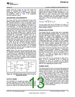
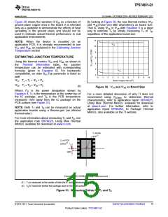
Knowing the maximum RθJA, the minimum amount of
PCB copper area needed for appropriate heatsinking
can be estimated using Figure 29.
temperature until thermal protection is triggered; use
worst-case loads and signal conditions. For good
reliability, thermal protection should trigger at least
+40°C above the maximum expected ambient
condition of the application. This condition produces a
worst-case junction temperature of +125°C at the
140
120
100
80
highest
worst-case load.
expected
ambient
temperature
and
The internal protection circuitry of the TPS74801-Q1
is designed to protect against overload conditions. It
is not intended to replace proper heatsinking.
Continuously running the TPS74801-Q1 into thermal
shutdown degrades device reliability.
60
40
20
LAYOUT RECOMMENDATIONS AND POWER
DISSIPATION
0
0
1
2
3
4
5
6
7
8
9
10
Board Copper Area (in2)
An optimal layout can greatly improve transient
performance, PSRR, and noise. To minimize the
voltage drop on the input of the device during load
transients, the capacitance on IN and BIAS should be
connected as close as possible to the device. This
capacitance also minimizes the effects of parasitic
inductance and resistance of the input source and
can, therefore, improve stability. To achieve optimal
transient performance and accuracy, the top side of
Note: θJA value at board size of 9in2 (that is, 3in ×
3in) is a JEDEC standard.
Figure 29. θJA vs Board Size
14
Submit Documentation Feedback
© 2010–2011, Texas Instruments Incorporated
Product Folder Link(s): TPS74801-Q1

 TI [ TEXAS INSTRUMENTS ]