TPS74801-Q1
www.ti.com
SLVSAI4A –OCTOBER 2010–REVISED FEBRUARY 2011
rapidly pulse the enable pin and still require the
device to soft-start from ground. CSS must be
low-leakage; X7R, X5R, or C0G dielectric materials
are preferred. Refer to Table 2 for suggested
soft-start capacitor values.
0.001μF soft-start capacitor, the output noise is
reduced by half and is typically 30μVRMS for a 1.2V
output (10Hz to 100kHz). Further increasing CSS has
little effect on noise. Because most of the output
noise is generated by the internal reference, the
noise is a function of the set output voltage. The RMS
noise with a 0.001μF soft-start capacitor is given in
Equation 3:
SEQUENCING REQUIREMENTS
VIN, VBIAS, and VEN can be sequenced in any order
without causing damage to the device. However, for
the soft-start function to work as intended, certain
sequencing rules must be applied. Connecting EN to
IN is acceptable for most applications, as long as VIN
is greater than 1.1V and the ramp rate of VIN and
VBIAS is faster than the set soft-start ramp rate. If the
ramp rate of the input sources is slower than the set
soft-start time, the output tracks the slower supply
minus the dropout voltage until it reaches the set
output voltage. If EN is connected to BIAS, the device
soft-starts as programmed, provided that VIN is
present before VBIAS. If VBIAS and VEN are present
before VIN is applied and the set soft-start time has
expired, then VOUT tracks VIN. If the soft-start time has
not expired, the output tracks VIN until VOUT reaches
the value set by the charging soft-start capacitor.
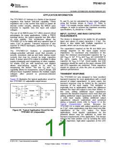
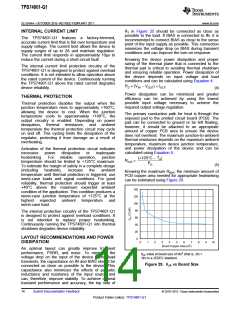
Figure 28 shows the use of an RC-delay circuit to
hold off VEN until VBIAS has ramped. This technique
can also be used to drive EN from VIN. An external
control signal can also be used to enable the device
after VIN and VBIAS are present.
mVRMS
VN(mVRMS) = 25
x VOUT(V)
(
)
V
(3)
The low output noise of the TPS74801-Q1 makes it a
good choice for powering transceivers, PLLs, or other
noise-sensitive circuitry.
ENABLE/SHUTDOWN
The enable (EN) pin is active high and is compatible
with standard digital signaling levels. VEN below 0.4V
turns the regulator off, while VEN above 1.1V turns the
regulator on. Unlike many regulators, the enable
circuitry has hysteresis and deglitching for use with
relatively slowly ramping analog signals. This
configuration allows the TPS74801-Q1 to be enabled
by connecting the output of another supply to the EN
pin. The enable circuitry typically has 50mV of
hysteresis and a deglitch circuit to help avoid on-off
cycling as a result of small glitches in the VEN signal.
The enable threshold is typically 0.8V and varies with
temperature and process variations. Temperature
variation is approximately –1mV/°C; process variation
accounts for most of the rest of the variation to the
0.4V and 1.1V limits. If precise turn-on timing is
required, a fast rise-time signal must be used to
enable the TPS74801-Q1.
NOTE: When VBIAS and VEN are present and VIN is
not supplied, this device outputs approximately 50μA
of current from OUT. Although this condition does not
cause any damage to the device, the output current
may charge up the OUT node if total resistance
between OUT and GND (including external feedback
resistors) is greater than 10kΩ.
If not used, EN can be connected to either IN or
BIAS. If EN is connected to IN, it should be
connected as close as possible to the largest
capacitance on the input to prevent voltage droops on
that line from triggering the enable circuit.
VIN
VOUT
IN
OUT
FB
R1
R2
CIN
COUT
BIAS
TPS74801
R
POWER GOOD
VBIAS
EN
SS
GND
CBIAS
The power good (PG) pin is an open-drain output and
can be connected to any 5.5V or lower rail through an
external pull-up resistor. This pin requires at least
1.1V on VBIAS in order to have a valid output. The PG
output is high-impedance when VOUT is greater than
VIT + VHYS. If VOUT drops below VIT or if VBIAS drops
below 1.9V, the open-drain output turns on and pulls
the PG output low. The PG pin also asserts when the
device is disabled. The recommended operating
condition of PG pin sink current is up to 1mA, so the
pull-up resistor for PG should be in the range of 10kΩ
to 1MΩ. If output voltage monitoring is not needed,
the PG pin can be left floating.
CSS
C
Figure 28. Soft-Start Delay Using an RC Circuit to
Enable the Device
OUTPUT NOISE
The TPS74801-Q1 provides low output noise when a
soft-start capacitor is used. When the device reaches
the end of the soft-start cycle, the soft-start capacitor
serves as a filter for the internal reference. By using a
© 2010–2011, Texas Instruments Incorporated
Submit Documentation Feedback
13
Product Folder Link(s): TPS74801-Q1

 TI [ TEXAS INSTRUMENTS ]