TPS65910, TPS65910A, TPS65910A3, TPS659101, TPS659102, TPS659103
TPS659104, TPS659105, TPS659106, TPS659107, TPS659108, TPS659109
SWCS046N –MARCH 2010–REVISED APRIL 2012
www.ti.com
Bits
Field Name
Description
Type
Reset
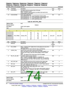
2
DCDCCKEXT
This signal control the muxing of the GPIO0 pad:
When 0: this pad is a GPIO
RW
0
When 1: this pad is used as input for an external clock used for the
synchronisation of the DCDCs
1:0
DCDCCKSYNC
DCDC clock configuration:
RW
0x3
DCDCCKSYNC[1:0] = 00 : no synchronization of DCDC clocks
DCDCCKSYNC[1:0] = 01 : DCDC synchronous clock with phase shift
DCDCCKSYNC[1:0] = 10 : no synchronization of DCDC clocks
DCDCCKSYNC[1:0] = 11 : DCDC synchronous clock
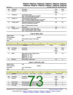
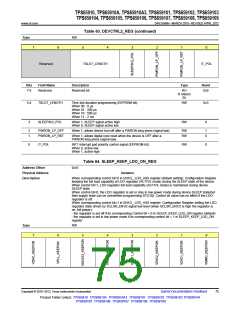
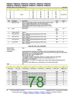
Table 62. DEVCTRL_REG
Address Offset
Physical Address
Description
Type
0x3F
Instance
Device control register
RW
7
6
5
4
3
2
1
0
Reserved
RTC_PWDN
CK32K_CTRL
DEV_ON
DEV_SLP
DEV_OFF
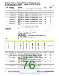
Bits
Field Name
Reserved
Description
Type
Reset
7
Reserved bit
RO
R returns
0s
0
6
5
RTC_PWDN
When 1, disable the RTC digital domain (clock gating and reset of RTC
registers and logic).
This register bit is not reset in BACKUP state. (EEPROM bit)
RW
1
0
CK32K_CTRL
Internal 32-kHz clock source control bit (EEPROM bit):
when 0, the internal 32-kHz clock source is the crystal oscillator or an
external 32-kHz clock in case the crystal oscillator is used in bypass
mode
RW
when 1, the internal 32-kHz clock source is the RC oscillator.
4
SR_CTL_I2C_SEL
Smartreflex registers access control bit:
RW
0
when 0: access to smartreflex registers by smartreflex I2C
when 1: access to smartreflex registers by control I2C The smartreflex
registers are: VDD1_OP_REG, VDD1_SR_REG, VDD2_OP_REG and
VDD2_SR_REG.
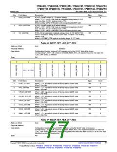
3
2
1
DEV_OFF_RST
DEV_ON
Write 1 will start an ACTIVE to OFF or SLEEP to OFF device state
transition (switch-off event) and activate reset of the digital core.
RW
RW
RW
0
0
0
Write 1 will maintain the device on (ACTIVE or SLEEP device state) (if
DEV_OFF = 0 and DEV_OFF_RST = 0).
DEV_SLP
Write 1 allows SLEEP device state (if DEV_OFF = 0 and
DEV_OFF_RST = 0).
Write ‘0’ will start an SLEEP to ACTIVE device state transition (wake-up
event) (if DEV_OFF = 0 and DEV_OFF_RST = 0). This bit is cleared in
OFF state.
0
DEV_OFF
Write 1 will start an ACTIVE to OFF or SLEEP to OFF device state
transition (switch-off event). This bit is cleared in OFF state.
RW
0
Table 63. DEVCTRL2_REG
Address Offset
Physical Address
Description
0x40
Instance
Device control register
74
Submit Documentation Feedback
Copyright © 2010–2012, Texas Instruments Incorporated
Product Folder Link(s): TPS65910 TPS65910A TPS65910A3 TPS659101 TPS659102 TPS659103 TPS659104
TPS659105 TPS659106 TPS659107 TPS659108 TPS659109

 TI [ TEXAS INSTRUMENTS ]