TPS65910, TPS65910A, TPS65910A3, TPS659101, TPS659102, TPS659103
TPS659104, TPS659105, TPS659106, TPS659107, TPS659108, TPS659109
www.ti.com
SWCS046N –MARCH 2010–REVISED APRIL 2012
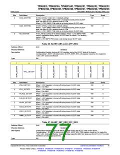
Bits
Field Name
Description
Type
Reset
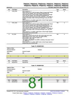
2
VDD2_KEEPON
If VDD2_EN1&2 control bit = 0 (default setting):
RW
0
When 1, VDD2 SMPS PWM mode is maintained during device SLEEP
state. No effect if VDD2 working mode is PFM.
When 0, VDD2 SMPS PFM mode is set during device SLEEP state.
1
0
VDD1_KEEPON
VIO_KEEPON
If VDD1_EN1&2 control bit=0 (default setting):
When 1, VDD1 SMPS PWM mode is maintained during device SLEEP
state. No effect if VDD1 working mode is PFM.
RW
RW
0
0
When 0, VDD1 SMPS PFM mode is set during device SLEEP state.
If VIO_EN1&2 control bit=0 (default setting): When 1, VIO SMPS PWM
mode is maintained during device SLEEP state. No effect if VIO working
mode is PFM.
When 0, VIO SMPS PFM mode is set during device SLEEP state.
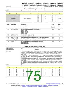
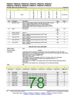
Table 66. SLEEP_SET_LDO_OFF_REG
Address Offset
Physical Address
Description
0x43
Instance
Configuration Register turning-off LDO regulator during the SLEEP state of the device.
Corresponding *_KEEP_ON control bit in SLEEP_KEEP_RES_ON register should be 0 to make this
*_SET_OFF control bit effective
Type
RW
7
6
5
4
3
2
1
0
VPLL_SETOFF
Bits
Field Name
Description
Type
Reset
7
VDAC_SETOFF
VPLL_SETOFF
VAUX33_SETOFF
IVAUX2_SETOFF
VAUX1_SETOFF
VDIG2_SETOFF
VDIG1_SETOFF
VMMC_SETOFF
When 1, LDO regulator is turned off during device SLEEP state.
When 0, No effect
RW
0
6
5
4
3
2
1
0
When 1, LDO regulator is turned off during device SLEEP state.
When 0, No effect
RW
RW
RW
RW
RW
RW
RW
0
0
0
0
0
0
0
When 1, LDO regulator is turned off during device SLEEP state.
When 0, No effect
When 1, LDO regulator is turned off during device SLEEP state.
When 0, No effect
When 1, LDO regulator is turned off during device SLEEP state.
When 0, No effect
When 1, LDO regulator is turned off during device SLEEP state.
When 0, No effect
When 1, LDO regulator is turned off during device SLEEP state.
When 0, No effect
When 1, LDO regulator is turned off during device SLEEP state.
When 0, No effect
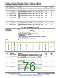
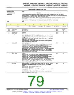
Table 67. SLEEP_SET_RES_OFF_REG
Address Offset
Physical Address
Description
0x44
Instance
Configuration Register turning-off SMPS regulator during the SLEEP state of the device.
Corresponding *_KEEP_ON control bit in SLEEP_KEEP_RES_ON2 register should be 0 to make this
*_SET_OFF control bit effective. Supplies voltage expected after their wake-up (SLEEP to ACTIVE state
transition) can also be programmed.
Type
RW
Copyright © 2010–2012, Texas Instruments Incorporated
Submit Documentation Feedback
77
Product Folder Link(s): TPS65910 TPS65910A TPS65910A3 TPS659101 TPS659102 TPS659103 TPS659104
TPS659105 TPS659106 TPS659107 TPS659108 TPS659109

 TI [ TEXAS INSTRUMENTS ]