TPS65910, TPS65910A, TPS65910A3, TPS659101, TPS659102, TPS659103
TPS659104, TPS659105, TPS659106, TPS659107, TPS659108, TPS659109
www.ti.com
SWCS046N –MARCH 2010–REVISED APRIL 2012
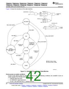
Any (not masked or masked) interrupt detection causes a POWER ON enable condition during a fixed delay
tDOINT1 (only) when the device is in OFF state (when NRESPWON signal is low). Any (not masked) interrupt
detection is causing a device wakeup from SLEEP state up to acknowledge of the pending interrupt. Any of the
interrupt sources can be masked by programming the INT_MSK_REG register. When an interrupt is masked, its
corresponding interrupt status bit is still updated, but the INT1 flag is not activated.
Interrupt source masking can be used to mask a device switch-on event. Because interrupt flag active is a
POWER ON enable condition during tDOINT1 delay, any interrupt not masked must be cleared to allow turn off of
the device after the tDOINT1 POWER ON enable pulse duration.. See section: Interrupts, for interrupt sources
definition.
SDASR_EN2 and SCLSR_EN1
SDASR_EN2 and SCLSR_EN1 are the data and clock signals of the serial control interface (SR-I2C) dedicated
to SmartReflex applications. These signals can also be programmed to be used as enable signals of one or
several supplies, when the device is on (NRESPWRON high). A resource assigned to SDASR_EN2 or
SCLSR_EN1 control automatically disables the serial control interface.
Programming EN1_LDO_ASS_REG, EN2_LDO_REG, and SLEEP_KEEP_LDO_ON_REG registers:
SCLSR_EN1 and SDASR_EN2 signals can be used to control the turn on/off or sleep state of any LDO type
supplies.
Programming EN1_SMPS_ASS_REG, EN2_SMPS_ASS_REG, and SLEEP_KEEP_RES_ON registers:
SCLSR_EN1 and SDASR_EN2 signals can be used to control the turn on/off or low-power state (PFM mode) of
SMPS type supplies.
SDASR_EN2 and SCLSR_EN1 can be used to set output voltage of VDD1 and VDD2 SMPS from a roof to a
floor value, preprogrammed in the VDD1_OP_REG, VDD2_OP_REG, and teh VDD1_SR_REG, VDD2_SR_REG
registers. Tun-off of VDD1 and VDD2 can also be programmed either in VDD1_OP_REG, VDD2_OP_REG or in
VDD1_SR_REG, VDD2_SR_REG registers.
When a supply is controlled through SCLSR_EN1 or SCLSR_EN2 signals, its state is no longer driven by the
device SLEEP state.
GPIO_CKSYNC
GPIO_CKSYNC is a configurable open-drain digital I/O: directivity, debouncing delay and internal pullup can be
programmed in the GPIO0_REG register. GPIO_CKSYNC cannot be used to turn on the device (OFF-to-ACTIVE
state transition), even if its associated interrupt is not masked, but can be used as an interrupt source to wake up
the device from SLEEP-to-ACTIVE state.
Programming DCDCCKEXT = 1, VDD1, VDD2, VIO, and VDD3 dc-dc switching can be synchronized using a 3-
MHz clock set though the GPIO_CKSYNC pin.
DYNAMIC VOLTAGE FREQUENCY SCALING AND ADAPTIVE VOLTAGE SCALING OPERATION
Dynamic voltage frequency scaling (DVFS) operation: a supply voltage value corresponding to a targeted
frequency of the digital core supplied is programmed in VDD1_OP_REG or VDD2_OP_REG registers.
The slew rate of the voltage supply reaching a new VDD1_OP_REG or VDD2_OP_REG programmed value is
limited to 12.5 mV/µs, fixed value. Adaptative voltage scaling (AVS) operation: a supply voltage value
corresponding to a supply voltage adjustment is programmed in VDD1_SR_REG or VDD2_SR_REG registers.
The supply voltage is then intended to be tuned by the digital core supplied, based its performance self-
evaluation. The slew rate of VDD1 or VDD2 voltage supply reaching a new programmed value is programmable
though the VDD1_REG or VDD2_REG register, respectively.
A serial control interface (SR-I2C) is dedicated to SmartReflex applications such as DVFS and class 3 AVS, and
thus gives access to the VDD1_OP_REG, VDD1_SR_REG, and VDD2_OP_REG, VDD2_SR_REG register.
A general-purpose serial control interface (CTL-I2C) also gives access to these registers, if SR_CTL_I2C_SEL
control bit is set to 1 in the DEVCTRL_REG register (default inactive).
Both control interfaces are compliant with HS-I2C specification (100 kbps, 400 kbps, or 3.4 Mbps).
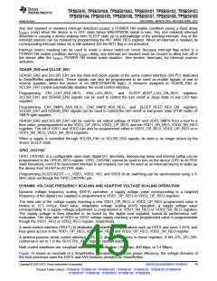
Figure 14 shows an example of a SmartReflex operation. To optimize power efficiency, the voltage domains of
the host processor uses the DVFS and AVS features provided by SmartReflex.
Copyright © 2010–2012, Texas Instruments Incorporated
Submit Documentation Feedback
45
Product Folder Link(s): TPS65910 TPS65910A TPS65910A3 TPS659101 TPS659102 TPS659103 TPS659104
TPS659105 TPS659106 TPS659107 TPS659108 TPS659109

 TI [ TEXAS INSTRUMENTS ]