TPS65910, TPS65910A, TPS65910A3, TPS659101, TPS659102, TPS659103
TPS659104, TPS659105, TPS659106, TPS659107, TPS659108, TPS659109
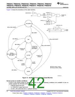
SWCS046N –MARCH 2010–REVISED APRIL 2012
www.ti.com
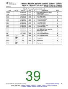
DEVICE INFORMATION
Table 11. Terminal Functions
NAME
VDDIO
QFN PIN
SUPPLIES
TYPE
I/O
DESCRIPTION
PU/PD
VDDIO/DGND
Power
I
Digital I/Os supply
No
I2C bidirectional data signal/serial
peripheral interface data input
(multiplexed)
I2C bidirectional clock signal/serial
peripheral interface Clock Input
(multiplexed)
SDA_SDI
SCL_SCK
VDDIO/DGND
VDDIO/DGND
Digital
Digital
I/O
I/O
External PU
External PU
I2C SmartReflex bidirectional data
signal/enable of supplies (multiplexed)
I2C SmartReflex bidirectional clock
signal/enable of supplies (multiplexed)
SDASR_EN2
SCLSR_EN1
SLEEP
VDDIO/DGND
VDDIO/DGND
VDDIO/DGND
Digital
Digital
Digital
I/O
I/O
I
External PU
External PU
Active-sleep state transition control
signal
Programmable PD
(default active)
Configurable general-purpose I/O or
DC-DCs synchronization clock input
signal
Programmable PD
(default active)
GPIO_CKSYNC
VDDIO/DGND
Digital
I/O
Programmable PD
(default active)
PWRHOLD
PWRON
VRTC/DGND
VBAT/DGND
Digital
Digital
I
I
Switch-on/-off control signal
Programmable PU
(default active)
External switch-on control (ON button)
PD active during
device OFF state
NRESPWRON
INT1
VDDIO/DGND
VDDIO/DGND
VRTC/DGND
Digital
Digital
Digital
O
O
I
Power off reset
Interrupt flag
No
Programmable PD
(default active)
BOOT0
Power-up sequence selection
Programmable PD
(default active)
BOOT1
VRTC/DGND
VDDIO/DGND
Digital
Digital
I
Power-up sequence selection
32-kHz clock output
PD disable in
ACTIVE or SLEEP
state
CLK32KOUT
O
OSC32KIN
OSC32KOUT
VREF
VRTC/REFGND
VRTC/REFGND
VCC7/REFGND
REFGND
Analog
Analog
Analog
Analog
Analog
I
I
32-kHz crystal oscillator
32-kHz crystal oscillator
Bandgap voltage
No
No
No
No
No
O
I/O
O
REFGND
TESTV
Reference ground
VCC7/AGND
Analog test output (DFT)
Backup battery input (short to VCC5 if
not used)
VBACKUP
VBACKUP/AGND
Power
I
No
VCC1
GND1
SW1
VCC1/GND1
VCC1/GND1
VCC1/GND1
VCC7/AGND
VCC2/GND2
VCC2/GND2
VCC2/GND2
VCC4/AGND2
VCCIO/GNDIO
VCCIO/GNDIO
VCCIO/GNDIO
VCC7/AGND
VCC3/AGND2
VCC3/REFGND
Power
Power
Power
Analog
Power
Power
Power
Analog
Power
Power
Power
Analog
Power
Power
I
I/O
O
I
VDD1 dc-dc power input
VDD1 dc-dc power ground
VDD1 dc-dc switched output
VDD1 feedback voltage
VDD2 dc-dc power input
VDD2 dc-dc power ground
VDD2 dc-dc switched output
VDD2 dc-dc feedback voltage
VIO dc-dc power input
No
No
No
PD
No
No
No
PD
No
No
No
PD
No
PD
VFB1
VCC2
GND2
SW2
I
I/O
O
I
VFB2
VCCIO
GNDIO
SWIO
VFBIO
VCC3
VMMC
I
I/O
O
I
VIO dc-dc power ground
VIO dc-dc switched output
VIO feedback voltage
I
VMMC VAUX33 power input
LDO regulator output
O
38
Submit Documentation Feedback
Copyright © 2010–2012, Texas Instruments Incorporated
Product Folder Link(s): TPS65910 TPS65910A TPS65910A3 TPS659101 TPS659102 TPS659103 TPS659104
TPS659105 TPS659106 TPS659107 TPS659108 TPS659109

 TI [ TEXAS INSTRUMENTS ]